Two-dimensional electron gas
A two-dimensional electron gas (2DEG) is a scientific model in solid-state physics. It is an electron gas that is free to move in two dimensions, but tightly confined in the third. This tight confinement leads to quantized energy levels for motion in the third direction, which can then be ignored for most problems. Thus the electrons appear to be a 2D sheet embedded in a 3D world. The analogous construct of holes is called a two-dimensional hole gas (2DHG), and such systems have many useful and interesting properties.
Realizations of 2DEG
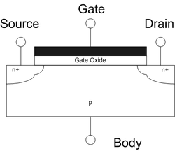


Most 2DEG are found in transistor-like structures made from semiconductors. The most commonly encountered 2DEG is the layer of electrons found in MOSFETs. When the transistor is in inversion mode, the electrons underneath the gate oxide are confined to the semiconductor-oxide interface, and thus occupy well defined energy levels. Nearly always, only the lowest level is occupied (see the figure caption), and so the motion of the electrons perpendicular to the interface can be ignored. However, the electron is free to move parallel to the interface, and so is quasi-two-dimensional.
Other methods for engineering 2DEGs are high-electron-mobility-transistors (HEMTs) and rectangular quantum wells. HEMTs are field-effect transistors that utilize the heterojunction between two semiconducting materials to confine electrons to a triangular quantum well. Electrons confined to the heterojunction of HEMTs exhibit higher mobilities than those in MOSFETs, since the former device utilizes an intentionally undoped channel thereby mitigating the deleterious effect of ionized impurity scattering. Two closely spaced heterojunction interfaces may be used to confine electrons to a rectangular quantum well. Careful choice of the materials and alloy compositions allow control of the carrier densities within the 2DEG.
Electrons may also be confined to the surface of a material. For example, free electrons will float on the surface of liquid helium, and are free to move along the surface, but stick to the helium; some of the earliest work in 2DEGs was done using this system.[1] Besides liquid helium, there are also solid insulators (such as topological insulators) that support conductive surface electronic states.
Recently, atomically thin solid materials have been developed (graphene, as well as metal dichalcogenide such as molybdenum disulfide) where the electrons are confined to an extreme degree. The two-dimensional electron system in graphene can be tuned to either a 2DEG or 2DHG by gating or chemical doping. This has been a topic of current research due to the versatile (some existing but mostly envisaged) applications of graphene.[2]
A separate class of heterostructures that can host 2DEGs are oxides. Although both sides of the heterostructure are insulators, the 2DEG at the interface may arise even without doping (which is the usual approach in semiconductors). Typical example is a ZnO/ZnMgO heterostructure.[3] More examples can be found in a recent review[4] including a notable discovery of 2004, a 2DEG at the LaAlO3/SrTiO3 interface[5] which becomes superconducting at low temperatures. The origin of this 2DEG is still unknown, but it may be similar to modulation doping in semiconductors, with electric-field-induced oxygen vacancies acting as the dopants.
Experiments
Considerable research involving 2DEGs and 2DHGs has been done, and much continues to this day. 2DEGs offer a mature system of extremely high mobility electrons, especially at low temperatures. When cooled to 4 K, 2DEGs may have mobilities of the order of 1,000,000 cm2/Vs and lower temperatures can lead to further increase of still. Specially grown, state of the art heterostructures with mobilities around 30,000,000 cm2/(V·s) have been made.[6] These enormous mobilities offer a test bed for exploring fundamental physics, since besides confinement and effective mass, the electrons do not interact with the semiconductor very often, sometimes traveling several micrometers before colliding; this so-called mean free path can be estimated in the parabolic band approximation as


![{\displaystyle \ell =v_{F}\tau ={\sqrt {2\pi n}}{\frac {\hbar \mu }{e}}\approx 5.2\ \mu \mathrm {m} \times \mu \ [10^{6}\ \mathrm {cm^{2}/Vs} ]{\sqrt {n\ [10^{11}\ \mathrm {cm^{-2}} ]}}}](../I/m/fd9e22271e264d8c0ff3e090611e5862cef815f4.svg)
where is the electron density in the 2DEG. Note that typically depends on .[7] Mobilities of 2DHG systems are smaller than those of most 2DEG systems, in part due to larger effective masses of holes (few 1000 cm2/(V·s) can already be considered high mobility[8]).

Aside from being in practically every semiconductor device in use today, two dimensional systems allow access to interesting physics. The quantum Hall effect was first observed in a 2DEG,[9] which led to two Nobel Prizes, in 1985 and 1998. Spectrum of a laterally modulated 2DEG (a two-dimensional superlattice) subject to magnetic field B can be represented as the Hofstadter's butterfly, a fractal structure in the energy vs B plot, signatures of which were observed in transport experiments.[10] Many more interesting phenomena pertaining to 2DEG have been studied.[1]
Footnotes
- 1. Examples of more 2DEG physics. Full control of the 2DEG spin polarization was recently demonstrated.[11] Possibly, this could be relevant to quantum information technology. Wigner crystallization in magnetic field. Microwave-induced magnetoresistance oscillations discovered by R. G. Mani et al.[12] Possible existence of non-abelian quasiparticles in the fractional quantum Hall effect at filling factor 5/2.
References
- Weisbuch, C.; Vinter, B. (1991). Quantum Semiconductor Structures: Fundamentals and Applications. Academic Press. ISBN 0-12-742680-9.
- Davies, J. H. (1997). The Physics of Low-dimensional Semiconductors: An Introduction. Cambridge University Press. ISBN 0-521-48148-1.
- ↑ Sommer, W. T. (1964). "Liquid Helium as a Barrier to Electrons". Physical Review Letters. 12 (11): 271–273. Bibcode:1964PhRvL..12..271S. doi:10.1103/PhysRevLett.12.271.
- ↑ Novoselov, K. S.; Fal′ko, V. I.; Colombo, L.; Gellert, P. R.; Schwab, M. G.; Kim, K. (2012). "A roadmap for graphene". Nature. 490 (7419): 192–200. Bibcode:2012Natur.490..192N. doi:10.1038/nature11458.
- ↑ Kozuka (2011). "Insulating phase of a two-dimensional electron gas in MgxZn1–xO/ZnO heterostructures below ν=1/3". Physical Review B. 84: 033304. arXiv:1106.5605
 . Bibcode:2011PhRvB..84c3304K. doi:10.1103/PhysRevB.84.033304.
 - ↑ Hwang (2012). "Emergent phenomena at oxide interfaces". Nature Materials. 11: 103. Bibcode:2012NatMa..11..103H. doi:10.1038/nmat3223.
- ↑ Ohtomo; Hwang (2004). "A high-mobility electron gas at the LaAlO3/SrTiO3 heterointerface". Nature. 427: 423. Bibcode:2004Natur.427..423O. doi:10.1038/nature02308.
- ↑ Kumar, A.; Csáthy, G. A.; Manfra, M. J.; Pfeiffer, L. N.; West, K. W. (2010). "Nonconventional Odd-Denominator Fractional Quantum Hall States in the Second Landau Level". Physical Review Letters. 105 (24). arXiv:1009.0237. Bibcode:2010PhRvL.105x6808K. doi:10.1103/PhysRevLett.105.246808.
- ↑ Pan, W.; Masuhara, N.; Sullivan, N. S.; Baldwin, K. W.; West, K. W.; Pfeiffer, L. N.; Tsui, D. C. (2011). "Impact of Disorder on the Fractional Quantum Hall State". Physical Review Letters. 106 (20). arXiv:1109.6911. Bibcode:2011PhRvL.106t6806P. doi:10.1103/PhysRevLett.106.206806.
- ↑ Myronov, M.; Sawano, K.; Shiraki, Y.; Mouri, T.; Itoh, K.M. (2008). "Observation of high mobility 2DHG with very high hole density in the modulation doped strained Ge quantum well at room temperature". Physica E. 40 (6): 1935–1937. Bibcode:2008PhyE...40.1935M. doi:10.1016/j.physe.2007.08.142.
- ↑ von Klitzing, K.; Dorda, G.; Pepper, M. (1980). "New Method for High-Accuracy Determination of the Fine-Structure Constant Based on Quantized Hall Resistance". Physical Review Letters. 45 (6): 494–497. Bibcode:1980PhRvL..45..494K. doi:10.1103/PhysRevLett.45.494.
- ↑ Geisler, M. C.; Smet, J. H.; Umansky, V.; von Klitzing, K.; Naundorf, B.; Ketzmerick, R.; Schweizer, H. (2004). "Detection of a Landau Band-Coupling-Induced Rearrangement of the Hofstadter Butterfly". Physical Review Letters. 92 (25). Bibcode:2004PhRvL..92y6801G. doi:10.1103/PhysRevLett.92.256801.
- ↑ Phelps, C.; Sweeney, T.; Cox, R. T.; Wang, H. (2009). "Ultrafast Coherent Electron Spin Flip in a Modulation-Doped CdTe Quantum Well". Physical Review Letters. 102 (23). Bibcode:2009PhRvL.102w7402P. doi:10.1103/PhysRevLett.102.237402.
- ↑ Mani, R. G.; Smet, J. H.; von Klitzing, K.; Narayanamurti, V.; Johnson, W. B.; Umansky, V. (2002). "Zero-resistance states induced by electromagnetic-wave excitation in GaAs/AlGaAs heterostructures". Nature. 420 (6916): 646–650. Bibcode:2002Natur.420..646M. doi:10.1038/nature01277.