Buck converter
A buck converter (step-down converter) is a DC-to-DC power converter which steps down voltage (while stepping up current) from its input (supply) to its output (load). It is a class of switched-mode power supply (SMPS) typically containing at least two semiconductors (a diode and a transistor, although modern buck converters frequently replace the diode with a second transistor used for synchronous rectification) and at least one energy storage element, a capacitor, inductor, or the two in combination. To reduce voltage ripple, filters made of capacitors (sometimes in combination with inductors) are normally added to such a converter's output (load-side filter) and input (supply-side filter).[1]

Switching converters (such as buck converters) provide much greater power efficiency as DC-to-DC converters than linear regulators, which are simpler circuits that lower voltages by dissipating power as heat, but do not step up output current.[2]
Buck converters can be remarkably efficient (often higher than 90%), making them useful for tasks such as converting a computer's main (bulk) supply voltage (often 12V) down to lower voltages needed by USB, DRAM, the CPU (1.8V or less), etc.
Theory of operation


The basic operation of the buck converter has the current in an inductor controlled by two switches (usually a transistor and a diode). In the idealised converter, all the components are considered to be perfect. Specifically, the switch and the diode have zero voltage drop when on and zero current flow when off and the inductor has zero series resistance. Further, it is assumed that the input and output voltages do not change over the course of a cycle (this would imply the output capacitance as being infinite).
Concept
The conceptual model of the buck converter is best understood in terms of the relation between current and voltage of the inductor. Beginning with the switch open (off-state), the current in the circuit is zero. When the switch is first closed (on-state), the current will begin to increase, and the inductor will produce an opposing voltage across its terminals in response to the changing current. This voltage drop counteracts the voltage of the source and therefore reduces the net voltage across the load. Over time, the rate of change of current decreases, and the voltage across the inductor also then decreases, increasing the voltage at the load. During this time, the inductor stores energy in the form of a magnetic field. If the switch is opened while the current is still changing, then there will always be a voltage drop across the inductor, so the net voltage at the load will always be less than the input voltage source. When the switch is opened again (off-state), the voltage source will be removed from the circuit, and the current will decrease. The changing current will produce a change in voltage across the inductor, and now the inductor becomes a voltage source. The stored energy in the inductor's magnetic field supports current flow through the load. During this time, the inductor is discharging its stored energy into the rest of the circuit. If the switch is closed again before the inductor fully discharges (on-state), the voltage at the load will always be greater than zero.
Continuous mode
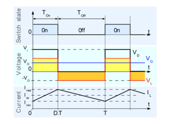
A buck converter operates in continuous mode if the current through the inductor () never falls to zero during the commutation cycle. In this mode, the operating principle is described by the plots in figure 4:

- When the switch pictured above is closed (top of figure 2), the voltage across the inductor is . The current through the inductor rises linearly. As the diode is reverse-biased by the voltage source V, no current flows through it;
- When the switch is opened (bottom of figure 2), the diode is forward biased. The voltage across the inductor is (neglecting diode drop). Current decreases.


The energy stored in inductor L is

Therefore, it can be seen that the energy stored in L increases during on-time as increases and then decreases during the off-state. L is used to transfer energy from the input to the output of the converter.
The rate of change of can be calculated from:

With equal to during the on-state and to during the off-state. Therefore, the increase in current during the on-state is given by:


Where is a scalar called the Duty Cycle with a value between 0 and 1.

Conversely, the decrease in current during the off-state is given by:

If we assume that the converter operates in the steady state, the energy stored in each component at the end of a commutation cycle T is equal to that at the beginning of the cycle. That means that the current is the same at and at (figure 4).


So we can write from the above equations:

The above integrations can be done graphically. In figure 4, is proportional to the area of the yellow surface, and to the area of the orange surface, as these surfaces are defined by the inductor voltage (red lines). As these surfaces are simple rectangles, their areas can be found easily: for the yellow rectangle and for the orange one. For steady state operation, these areas must be equal.


As can be seen in figure 4, and .


This yields:

From this equation, it can be seen that the output voltage of the converter varies linearly with the duty cycle for a given input voltage. As the duty cycle is equal to the ratio between and the period , it cannot be more than 1. Therefore, . This is why this converter is referred to as step-down converter.


So, for example, stepping 12 V down to 3 V (output voltage equal to one quarter of the input voltage) would require a duty cycle of 25%, in our theoretically ideal circuit.
Discontinuous mode
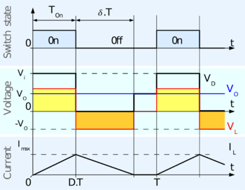
In some cases, the amount of energy required by the load is too small. In this case, the current through the inductor falls to zero during part of the period. The only difference in the principle described above is that the inductor is completely discharged at the end of the commutation cycle (see figure 5). This has, however, some effect on the previous equations.
The inductor current falling below zero results in the discharging of the output capacitor during each cycle and therefore higher switching losses. A different control technique known as Pulse-frequency modulation can be used to minimize these losses.
We still consider that the converter operates in steady state. Therefore, the energy in the inductor is the same at the beginning and at the end of the cycle (in the case of discontinuous mode, it is zero). This means that the average value of the inductor voltage (VL) is zero; i.e., that the area of the yellow and orange rectangles in figure 5 are the same. This yields:

So the value of δ is:

The output current delivered to the load () is constant, as we consider that the output capacitor is large enough to maintain a constant voltage across its terminals during a commutation cycle. This implies that the current flowing through the capacitor has a zero average value. Therefore, we have :


Where is the average value of the inductor current. As can be seen in figure 5, the inductor current waveform has a triangular shape. Therefore, the average value of IL can be sorted out geometrically as follow:


The inductor current is zero at the beginning and rises during ton up to ILmax. That means that ILmax is equal to:

Substituting the value of ILmax in the previous equation leads to:

And substituting δ by the expression given above yields:

This expression can be rewritten as:

It can be seen that the output voltage of a buck converter operating in discontinuous mode is much more complicated than its counterpart of the continuous mode. Furthermore, the output voltage is now a function not only of the input voltage (Vi) and the duty cycle D, but also of the inductor value (L), the commutation period (T) and the output current (Io).
From discontinuous to continuous mode (and vice versa)
As mentioned at the beginning of this section, the converter operates in discontinuous mode when low current is drawn by the load, and in continuous mode at higher load current levels. The limit between discontinuous and continuous modes is reached when the inductor current falls to zero exactly at the end of the commutation cycle. Using the notations of figure 5, this corresponds to :

Therefore, the output current (equal to the average inductor current) at the limit between discontinuous and continuous modes is (see above):

Substituting ILmax by its value:

On the limit between the two modes, the output voltage obeys both the expressions given respectively in the continuous and the discontinuous sections. In particular, the former is

So Iolim can be written as:

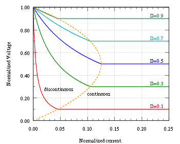
Let's now introduce two more notations:
- the normalized voltage, defined by . It is zero when , and 1 when ;
- the normalized current, defined by . The term is equal to the maximum increase of the inductor current during a cycle; i.e., the increase of the inductor current with a duty cycle D=1. So, in steady state operation of the converter, this means that equals 0 for no output current, and 1 for the maximum current the converter can deliver.


Using these notations, we have:
- in continuous mode:
- in discontinuous mode:


the current at the limit between continuous and discontinuous mode is:

Therefore, the locus of the limit between continuous and discontinuous modes is given by:

These expressions have been plotted in figure 6. From this, it is obvious that in continuous mode, the output voltage does only depend on the duty cycle, whereas it is far more complex in the discontinuous mode. This is important from a control point of view.
Non-ideal circuit

The previous study was conducted with the following assumptions:
- The output capacitor has enough capacitance to supply power to the load (a simple resistance) without any noticeable variation in its voltage.
- The voltage drop across the diode when forward biased is zero
- No commutation losses in the switch nor in the diode
These assumptions can be fairly far from reality, and the imperfections of the real components can have a detrimental effect on the operation of the converter.
Output voltage ripple
Output voltage ripple is the name given to the phenomenon where the output voltage rises during the On-state and falls during the Off-state. Several factors contribute to this including, but not limited to, switching frequency, output capacitance, inductor, load and any current limiting features of the control circuitry. At the most basic level the output voltage will rise and fall as a result of the output capacitor charging and discharging:

During the Off-state, the current in this equation is the load current. In the On-state the current is the difference between the switch current (or source current) and the load current. The duration of time (dT) is defined by the duty cycle and by the switching frequency.
For the On-state:

For the Off-state:

Qualitatively, as the output capacitor or switching frequency increase, the magnitude of the ripple decreases. Output voltage ripple is typically a design specification for the power supply and is selected based on several factors. Capacitor selection is normally determined based on cost, physical size and non-idealities of various capacitor types. Switching frequency selection is typically determined based on efficiency requirements, which tends to decrease at higher operating frequencies, as described below in Effects of non-ideality on the efficiency. Higher switching frequency can also reduce efficiency and possibly raise EMI concerns.
Output voltage ripple is one of the disadvantages of a switching power supply, and can also be a measure of its quality.
Effects of non-ideality on the efficiency
A simplified analysis of the buck converter, as described above, does not account for non-idealities of the circuit components nor does it account for the required control circuitry. Power losses due to the control circuitry are usually insignificant when compared with the losses in the power devices (switches, diodes, inductors, etc.) The non-idealities of the power devices account for the bulk of the power losses in the converter.
Both static and dynamic power losses occur in any switching regulator. Static power losses include (conduction) losses in the wires or PCB traces, as well as in the switches and inductor, as in any electrical circuit. Dynamic power losses occur as a result of switching, such as the charging and discharging of the switch gate, and are proportional to the switching frequency.

It is useful to begin by calculating the duty cycle for a non-ideal buck converter, which is:

where:
- VSWITCH is the voltage drop on the power switch,
- VSYNCSW is the voltage drop on the synchronous switch or diode, and
- VL is the voltage drop on the inductor.
The voltage drops described above are all static power losses which are dependent primarily on DC current, and can therefore be easily calculated. For a diode drop, VSWITCH and VSYNCHSW may already be known, based on the properties of the selected device.


where:
- Ron is the ON-resistance of each switch, and
- RDCR is the DC resistance of the inductor.
The duty cycle equation is somewhat recursive. A rough analysis can be made by first calculating the values VSWITCH and VSYNCSW using the ideal duty cycle equation.
For a MOSFET voltage drop, a common approximation is to use Rds(on) from the MOSFET's datasheet in Ohm's Law, V = Ids*Rdson(sat). This approximation is acceptable because the MOSFET is in the linear state, with a relatively constant drain-source resistance. This approximation is only valid at relatively low Vds values. For more accurate calculations, MOSFET datasheets contain graphs on the Vds and Ids relationship at multiple Vgs values. Observe Vds at the Vgs and Ids which most closely match what is expected in the buck converter.[3]
In addition, power loss occurs as a result of leakage currents. This power loss is simply

where:
- Ileakage is the leakage current of the switch, and
- V is the voltage across the switch.
Dynamic power losses are due to the switching behavior of the selected pass devices (MOSFETs, power transistors, IGBTs, etc.). These losses include turn-on and turn-off switching losses and switch transition losses.
Switch turn-on and turn-off losses are easily lumped together as

where:
- V is the voltage across the switch while the switch is off,
- trise and tfall are the switch rise and fall times, and
- T is the switching period.
But this doesn't take into account the parasitic capacitance of the MOSFET which makes the Miller plate. Then, the switch losses will be more like:

When a MOSFET is used for the lower switch, additional losses may occur during the time between the turn-off of the high-side switch and the turn-on of the low-side switch, when the body diode of the low-side MOSFET conducts the output current. This time, known as the non-overlap time, prevents "shootthrough", a condition in which both switches are simultaneously turned on. The onset of shootthrough generates severe power loss and heat. Proper selection of non-overlap time must balance the risk of shootthrough with the increased power loss caused by conduction of the body diode. Many MOSFET based buck converters also include a diode to aid the lower MOSFET body diode with conduction during the non-overlap time. When a diode is used exclusively for the lower switch, diode forward turn-on time can reduce efficiency and lead to voltage overshoot.[4]
Power loss on the body diode is also proportional to switching frequency and is

where:
- VF is the forward voltage of the body diode, and
- tno is the selected non-overlap time.
Finally, power losses occur as a result of the power required to turn the switches on and off. For MOSFET switches, these losses are dominated by the gate charge, essentially the energy required to charge and discharge the capacitance of the MOSFET gate between the threshold voltage and the selected gate voltage. These switch transition losses occur primarily in the gate driver, and can be minimized by selecting MOSFETs with low gate charge, by driving the MOSFET gate to a lower voltage (at the cost of increased MOSFET conduction losses), or by operating at a lower frequency.

where:
- QG is the gate charge of the selected MOSFET, and
- VGS is the peak gate-source voltage.
It is essential to remember that, for N-MOSFETs, the high-side switch must be driven to a higher voltage than Vi. To achieve this, MOSFET gate drivers typically feed the MOSFET output voltage back into the gate driver. The gate driver then adds its own supply voltage to the MOSFET output voltage when driving the high-side MOSFETs to achieve a Vgs equal to the gate driver supply voltage.[5] Because the low-side Vgs is the gate driver supply voltage, this results in very similar Vgs values for high-side and low-side MOSFETs.
A complete design for a buck converter includes a tradeoff analysis of the various power losses. Designers balance these losses according to the expected uses of the finished design. A converter expected to have a low switching frequency does not require switches with low gate transition losses; a converter operating at a high duty cycle requires a low-side switch with low conduction losses.
Specific structures
Synchronous rectification
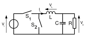
A synchronous buck converter is a modified version of the basic buck converter circuit topology in which the diode, D, is replaced by a second switch, S2. This modification is a tradeoff between increased cost and improved efficiency.
In a standard buck converter, the flyback diode turns on, on its own, shortly after the switch turns off, as a result of the rising voltage across the diode. This voltage drop across the diode results in a power loss which is equal to

where:
- VD is the voltage drop across the diode at the load current Io,
- D is the duty cycle, and
- Io is the load current.
By replacing diode D with switch S2, which is advantageously selected for low losses, the converter efficiency can be improved. For example, a MOSFET with very low RDSON might be selected for S2, providing power loss on switch 2 which is

In both cases, power loss is strongly dependent on the duty cycle, D. Power loss on the freewheeling diode or lower switch will be proportional to its on-time. Therefore, systems designed for low duty cycle operation will suffer from higher losses in the freewheeling diode or lower switch, and for such systems it is advantageous to consider a synchronous buck converter design.
Without actual numbers the reader will find the usefulness of this substitution to be unclear. Consider a computer power supply, where the input is 5 V, the output is 3.3 V, and the load current is 10A. In this case, the duty cycle will be 66% and the diode would be on for 34% of the time. A typical diode with forward voltage of 0.7 V would suffer a power loss of 2.38 W. A well-selected MOSFET with RDSON of 0.015 Ω, however, would waste only 0.51 W in conduction loss. This translates to improved efficiency and reduced heat loss.
Another advantage of the synchronous converter is that it is bi-directional, which lends itself to applications requiring regenerative braking. When power is transferred in the "reverse" direction, it acts much like a boost converter.
The advantages of the synchronous buck converter do not come without cost. First, the lower switch typically costs more than the freewheeling diode. Second, the complexity of the converter is vastly increased due to the need for a complementary-output switch driver.
Such a driver must prevent both switches from being turned on at the same time, a fault known as "shootthrough". The simplest technique for avoiding shootthrough is a time delay between the turn-off of S1 to the turn-on of S2, and vice versa. However, setting this time delay long enough to ensure that S1 and S2 are never both on will itself result in excess power loss. An improved technique for preventing this condition is known as adaptive "non-overlap" protection, in which the voltage at the switch node (the point where S1, S2 and L are joined) is sensed to determine its state. When the switch node voltage passes a preset threshold, the time delay is started. The driver can thus adjust to many types of switches without the excessive power loss this flexibility would cause with a fixed non-overlap time.
Multiphase buck
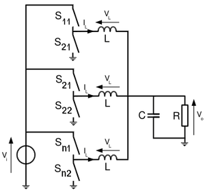
The multiphase buck converter is a circuit topology where basic buck converter circuits are placed in parallel between the input and load. Each of the n "phases" is turned on at equally spaced intervals over the switching period. This circuit is typically used with the synchronous buck topology, described above.
This type of converter can respond to load changes as quickly as if it switched n times faster, without the increase in switching losses that would cause. Thus, it can respond to rapidly changing loads, such as modern microprocessors.
There is also a significant decrease in switching ripple. Not only is there the decrease due to the increased effective frequency,[6] but any time that n times the duty cycle is an integer, the switching ripple goes to 0; the rate at which the inductor current is increasing in the phases which are switched on exactly matches the rate at which it is decreasing in the phases which are switched off.
Another advantage is that the load current is split among the n phases of the multiphase converter. This load splitting allows the heat losses on each of the switches to be spread across a larger area.
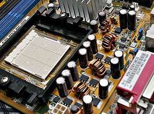
This circuit topology is used in computer motherboards to convert the 12 VDC power supply to a lower voltage (around 1 V), suitable for the CPU. Modern CPU power requirements can exceed 200W,[7] can change very rapidly, and have very tight ripple requirements, less than 10mV. Typical motherboard power supplies use 3 or 4 phases.
One major challenge inherent in the multiphase converter is ensuring the load current is balanced evenly across the n phases. This current balancing can be performed in a number of ways. Current can be measured "losslessly" by sensing the voltage across the inductor or the lower switch (when it is turned on). This technique is considered lossless because it relies on resistive losses inherent in the buck converter topology. Another technique is to insert a small resistor in the circuit and measure the voltage across it. This approach is more accurate and adjustable, but incurs several costs—space, efficiency and money.
Finally, the current can be measured at the input. Voltage can be measured losslessly, across the upper switch, or using a power resistor, to approximate the current being drawn. This approach is technically more challenging, since switching noise cannot be easily filtered out. However, it is less expensive than emplacing a sense resistor for each phase.
Efficiency factors
Conduction losses that depend on load:
- Resistance when the transistor or MOSFET switch is conducting.
- Diode forward voltage drop (usually 0.7 V or 0.4 V for schottky diode)
- Inductor winding resistance
- Capacitor equivalent series resistance
Switching losses:
- Voltage-Ampere overlap loss
- Frequencyswitch*CV2 loss
- Reverse latence loss
- Losses due driving MOSFET gate and controller consumption.
- Transistor leakage current losses, and controller standby consumption.[8]
Impedance matching
A buck converter can be used to maximize the power transfer through the use of impedance matching. An application of this is in a "maximum power point tracker" commonly used in photovoltaic systems.
By the equation for electric power:

where:
- Vo is the output voltage
- Io is the output current
- η is the power efficiency (ranging from 0 to 1)
- Vi is the input voltage
- Ii is the input current
By Ohm's Law:


where:
- Zo is the output impedance
- Zi is the input impedance
Substituting these expressions for Io and Ii into the power equation yields:

As was previously shown for the continuous mode, (where IL > 0):

where:
- D is the duty cycle
Substituting this equation for Vo into the previous equation, yields:

which reduces to:

and finally:

This shows that it is possible to adjust the impedance ratio by adjusting the duty cycle. This is particularly useful in applications where the impedance(s) are dynamically changing.
See also
- Boost converter
- Buck-boost converter
- Split-Pi (Boost-Buck Converter)
- General DC-DC converters and Switched-mode power supplies
References
- ↑ Mammano, Robert. "Switching power supply topology voltage mode vs. current mode." Elektron Journal-South African Institute of Electrical Engineers 18.6 (2001): 25-27.
- ↑ http://www.digikey.com/en/articles/techzone/2012/may/understanding-the-advantages-and-disadvantages-of-linear-regulators
- ↑ "Power MOSFET datasheet list". http://www.magnachip.com. MagnaChip. Retrieved 25 January 2015. External link in
|website=(help) - ↑ Jim Williams (1 January 2009). "Diode Turn-On Time Induced Failures in Switching Regulators".
- ↑ "NCP5911 datasheet" (PDF). http://www.onsemi.com. ON Semiconductor. Retrieved 25 January 2015. External link in
|website=(help) - ↑ Guy Séguier, Électronique de puissance, 7th edition, Dunod, Paris 1999 (in French)
- ↑ Tom's Hardware: "Idle/Peak Power Consumption Analysis"
- ↑ "iitb.ac.in - Buck converter" (PDF). 090424 ee.iitb.ac.in
| Wikimedia Commons has media related to Buck converters. |
- P. Julián, A. Oliva, P. Mandolesi, and H. Chiacchiarini, "Output discrete feedback control of a DC-DC Buck converter," in Proceedings of the IEEE International Symposium on Industrial Electronics (ISIE’97), Guimaraes, Portugal, 7-11Julio 1997, pp. 925–930.
- H. Chiacchiarini, P. Mandolesi, A. Oliva, and P. Julián, "Nonlinear analog controller for a buck converter: Theory and experimental results", Proceedings of the IEEE International Symposium on Industrial Electronics (ISIE’99), Bled, Slovenia, 12–16 July 1999, pp. 601–606.
- M. B. D’Amico, A. Oliva, E. E. Paolini y N. Guerin, "Bifurcation control of a buck converter in discontinuous conduction mode", Proceedings of the 1st IFAC Conference on Analysis and Control of Chaotic Systems (CHAOS’06), pp. 399–404, Reims (Francia), 28 al 30 de junio de 2006.
- Oliva, A.R., H. Chiacchiarini y G. Bortolotto "Developing of a state feedback controller for the synchronous buck converter", Latin American Applied Research, Volumen 35, Nro 2, Abril 2005, pp. 83–88. ISSN 0327-0793.
- D’Amico, M. B., Guerin, N., Oliva, A.R., Paolini, E.E. Dinámica de un convertidor buck con controlador PI digital. Revista Iberoamericana de automática e informática industrial (RIAI), Vol 4, No 3, julio 2007, pp. 126–131. ISSN 1697-7912.
- Chierchie, F. Paolini, E.E. Discrete-time modeling and control of a synchronous buck converter .Argentine School of Micro-Nanoelectronics, Technology and Applications, 2009. EAMTA 2009.1–2 October 2009, pp. 5 – 10 . ISBN 978-1-4244-4835-7 .
External links
- Interactive Power Electronics Seminar (iPES) Many Java applets demonstrating the operation of converters
- Model based control of digital buck converter Description and working VisSim source code diagram for low cost digital control of DC-DC buck converters
- SPICE simulation of the buck converter
- Tutorial video explaining buck converters with example buck converter circuit design
- Switch-Mode Power Supply Tutorial - Detailed article on DC-DC converters which gives a more formal and detailed analysis of the Buck including the effects of non-ideal switching (but, note that the diagram of the buck-boost converter fails to account for the inversion of the polarity of the voltage between input and output).
- DC-DC Power Converter Case study
- On the Power Efficiency Optimization
- Multiphase DC-DC converter