Eutectic bonding
Ultrasonic image of a blank Au-Si eutectic bonded wafer [1] |
 Ultrasonic image of a patterned Au-Si eutectic bonded wafer [1] |
Eutectic bonding, also referred to as eutectic soldering, describes a wafer bonding technique with an intermediate metal layer that can produce a eutectic system. Those eutectic metals are alloys that transform directly from solid to liquid state, or vice versa from liquid to solid state, at a specific composition and temperature without passing a two-phase equilibrium, i.e. liquid and solid state. The fact that the eutectic temperature can be much lower than the melting temperature of the two or more pure elements can be important in eutectic bonding.
Eutectic alloys are deposited by sputtering, dual source evaporation or electroplating. It also can be formed by diffusion reactions of pure materials and subsequently melting of the eutectic composition.[2]
Eutectic bonding is able to produce hermetically sealed packages and electrical interconnection within a single process (compare ultrasonic images). In addition this procedure is conducting at low processing temperatures, low resultant stress induced in final assembly, high bonding strength, large fabrication yield and a good reliability. Those attributes are dependent on the coefficient of thermal expansion between the substrates.[1]
The most important parameters for eutectic bonding are:
- bonding temperature
- bonding duration
- tool pressure
Overview
Eutectic bonding is based on the ability of silicon (Si) to alloy with numerous metals and form a eutectic system. The most established eutectic formations are Si with gold (Au) or with aluminium (Al).[3] This bonding procedure is most commonly used for Si or glass wafers that are coated with an Au/Al film and partly with adhesive layer (compare with following image).

The Si-Au couple has the advantages of an exceptionally low eutectic temperature, an already widespread use in die bonding and the compatibility with Al interconnects.[4] Additionally, often used eutectic alloys for wafer bonding in semiconductor fabrication are shown in the table. Choosing the correct alloy is determined by the processing temperature and compatibility of the materials used.[5]
| Eutectic alloy | Eutectic composition | Eutectic temperature |
|---|---|---|
| Au-In | 0.6 / 99.4 wt-% | 156 °C |
| Cu-Sn | 5 / 95 wt-% | 231 °C |
| Au-Sn[6] | 80 / 20 wt-% | 280 °C |
| Au-Ge | 72 / 28 wt-% | 361 °C |
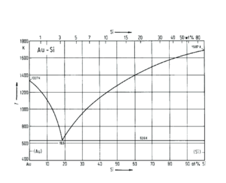
| Au-Si | 97.15 / 2.85 wt-% | 370 °C |
| Al-Ge[7] | 49 / 51 wt-% | 419 °C |
| Al-Si | 87.5 / 12.5 wt-% | 580 °C |
Further, the bonding has less restrictions, concerning substrate roughness and planarity than direct bonding. Compared to anodic bonding, no high voltages are required that can be detrimental to electrostatic MEMS. Additionally, the eutectic bonding procedure promotes a better out-gassing and hermeticity than bonding with organic intermediate layers.[8] Compared to glass frit bonding, the advantage sticks out that the reduction of seal ring geometries, an increase of the hermeticity levels and a shrinking of device size is possible. The geometry of eutectic seals is characterized by a thickness of 1 - 5 µm and a wideness of > 50 µm. The use of eutectic alloy brings the advantage of providing electrical conduction and interfacing with redistribution layers.
The temperature of the eutectic bonding procedure is dependent on the used material. The bonding happens at a specific weight-% and temperature, e.g. 370 °C at 2.85 wt-% Si for Au intermediate layer (compare to phase diagram).[3]
The procedure of eutectic bonding is divided into following steps:[9]
- Substrate processing
- Conditioning prior to bonding (e.g. oxide removal)
- Bonding process (Temperature, Mechanical Pressure for a few minutes)
- Cooling process
Procedural steps
Pre-treatment
The surface preparation is the most important step to accomplish a successful eutectic bonding. This bonding procedure is due to oxide presence on the silicon substrates very limited based on the poor wettability of Au on the oxide layer. This leads to a poor adhesion of the eutectic bond. The oxide on the silicon surface acts as a diffusion barrier.[4] The surface preparation's main task is to facilitate the deposition of the eutectic metal by oxide removal or adhesion layer deposition.[10]
To remove existing native oxide layers wet chemical etching (HF clean), dry chemical etching or chemical vapor deposition (CVD) with different types of crystals can be used. Also some applications require a surface pre-treatment using dry oxide removal processes, e.g. H2 plasma and CF4 plasma.[1]
An additional method for the removal of unwanted surface films, i.e. oxide, is applying ultrasound during attachment process.[11] As soon the tool is lowered a relative vibration between the wafer and the substrate is applied. Commonly, industrial bonders use ultrasonic with 60 Hz vibration frequencies and 100 µm vibration amplitude.[12] A successful oxide removal results in a solid, hermetically tight connection.[3]
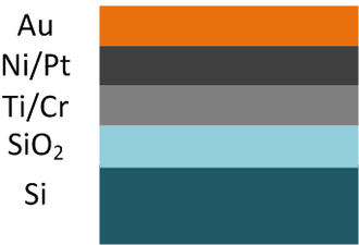
A Second method to ensure the eutectic metal adheres on the Si wafer is by using an adhesion layer. This thin intermediate metal layer adheres well to the oxide and the eutectic metal. Well suitable metals for an Au-Si compound are titanium (Ti) and chromium (Cr) resulting in, e.g. Si-SiO2-Ti-Au or Si-SiO2-Cr-Au. The adhesion layer is used to break up the oxide by diffusion of silicon into the used material. A typical wafer is composed of a silicon wafer with oxide, 30 - 200 nm Ti or Cr layer and Au layer of > 500 nm thickness.
In the wafer fabrication a nickel (Ni) or a platinum (Pt) layer is added between the gold and the substrate wafer as diffusion barrier.[8] The diffusion barrier avoids interaction between Au and Ti/Cr and requires higher temperatures to form a reliable and uniform bond. Further, the very limited solubility of silicon in titanium and chromium can prevent the developing of Au-Si eutectic composition based on the diffusion of silicon through titanium into gold.[4]
The eutectic materials and optional adhesion layers are usually approached by deposition as alloy in one layer by dual component electroplating, dual-source evaporation (physical vapor deposition) or composite alloy sputtering.[10]
The removal of contamination, on the for silicon most established Au layer, is usually realized with water flushing and wafer heating.[1]
Bonding process
The contacting of the substrates is applied directly after the pre-treatment of the surfaces to avoid oxide regeneration. The bonding procedure for oxidizing metals (not Au) generally takes place in a reduced atmosphere of 4% hydrogen and an inert carrier gas flow, e.g. nitrogen. The requirements for the bonding equipment lies in the thermal and pressure uniformity across the wafer. This enables uniformly compressed seal lines.[2]
The substrate is aligned and fixed on a heated stage and the silicon wafer in a heated tool. The substrates inserted in the bonding chamber are contacted maintaining the alignment. As soon the layers are in atomic contact the reaction between those starts. To support the reaction mechanical pressure is applied and heating above the eutectic temperature is carried out.[1]
The diffusivity and solubility of gold into silicon substrate increases with rising bonding temperatures. A higher temperature than the eutectic temperature is usually preferred for the bonding procedure. This may result in the formation of a thicker Au-Si alloy layer and further a stronger eutectic bond.[13]
The diffusion starts as soon as the layers are in atomic contact at elevated temperatures.[1] The contacted surface layer containing the eutectic composites melts, forming a liquid phase alloy, accelerating further mixing processes and diffusion until the saturation composition is reached.[14][15]
Other common eutectic bonding alloys commonly used for wafer bonding include Au-Sn, Al-Ge, Au-Ge, Au-In and Cu-Sn.[7]
The chosen bonding temperature usually is some degrees higher than the eutectic temperature so the melt becomes less viscous and readily flows due to higher roughness to surface areas that are not in atomic contact.[10] To prevent the melt pressed outside the bonding interface the optimization of the bonding parameter control is necessary, e.g. low force on the wafers. Otherwise, it may lead to short circuits or device malfunctions of the used components (electrical and mechanical).[1] The heating of the wafers leads to a change in the surface texture due to formation of fine silicon micro structures on top of the gold surface.[15]
Cooling process
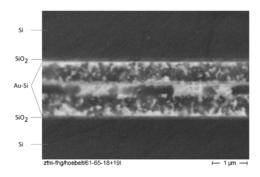
The material mix is solidified when the temperature decreases below eutectic point or the concentration ratio changes (for Si-Au: T < 370 °C).[1] The solidification leads to epitaxial growth of silicon and gold on top of the silicon substrate resulting in numerous small silicon islands protruding from a polycrystalline gold alloy (compare to cross-section image of the bonding interface).[4] This can result in bonding strengths around 70 MPa.
The importance lies in the appropriate process parameters, i.e. sufficient bonding temperature control.[15] Otherwise the bond cracks due to stress caused by a mismatch of the thermal expansion coefficient. This stress is able to relax over time.[4]
Examples
Based on the high bonding strength this procedure is special applicable for pressure sensors or fluidics. Also smart micro mechanical sensors and actuators with electronic and/or micro mechanical functions over multiple wafers can be fabricated.[15]
Technical specifications
| Materials |
Substrate:
Intermediate layer:
|
| Temperature |
|
| Advantages |
|
| Drawbacks |
|
| Researches |
|
References
- 1 2 3 4 5 6 7 8 9 10 11 Lin, Y.-C.; Baum M.; Haubold, M.; Fromel J.; Wiemer, M.; Gessner T.; Esashi, M. (2009). "Development and evaluation of AuSi eutectic wafer bonding". Solid-State Sensors, Actuators and Microsystems Conference, 2009. TRANSDUCERS 2009. International. pp. 244–247. doi:10.1109/SENSOR.2009.5285519.
- 1 2 Farrens, S.; Sood, S. (2008). "Wafer Level Packaging: Balancing Device Requirements and Materials Properties". IMAPS. International Microelectronics and Packaging Society. SUSS MicroTec.
- 1 2 3 4 G. Gerlach; W. Dötzel (2008). Ronald Pething, ed. Introduction to Microsystem Technology: A Guide for Students (Wiley Microsystem and Nanotechnology). Wiley Publishing. ISBN 978-0-470-05861-9.
- 1 2 3 4 5 R. F. Wolffenbuttel (1997). "Low-temperature intermediate Au-Si wafer bonding; eutectic or silicide bond". Sensors and Actuators A: Physical. 62 (1-3). pp. 680–686.
- ↑ Farrens, S. (2008). Latest Metal Technologies for 3D Integration and MEMS Wafer Level Bonding (Report). SUSS MicroTec Inc.
- ↑ Matijasevic, G.S.; Lee C.C.; Wang, C.Y. (1993). "Au-Sn alloy phase diagram and properties related to its use as a bonding medium". Thin Solid Films. 223. pp. 276–287.
- 1 2 Sood, S.; Farrens S.; Pinker, R.; Xie J.; Cataby, W. (2010). "Al-Ge Eutectic Wafer Bonding and Bond Characterization for CMOS Compatible Wafer Packaging". ECS Transactions. 33. pp. 93–101.
- 1 2 Lani, S.; Bosseboeuf, A.; Belier, B.; Clerc, C.; Gousset, C.; Aubert, J. (2006). "Gold metallizations for eutectic bonding of silicon wafers". Microsystem Technologies. 12. pp. 1021–1025. doi:10.1007/s00542-006-0228-6.
- ↑ M. Wiemer; J. Frömel; T. Gessner (2003). "Trends der Technologieentwicklung im Bereich Waferbonden". In W. Dötzel. 6. Chemnitzer Fachtagung Mikromechanik & Mikroelektronik. 6. Technische Universität Chemnitz. Technische Universität Chemnitz. pp. 178–188.
- 1 2 3 Farrens, S. (2008). Tan, C. S.; Gutmann, R. J.; Reif, L. R., eds. "Wafer-Bonding Technologies and Strategies for 3D ICs. Chapter 4". Integrated Circuits and Systems. Springer US. pp. 49–85. doi:10.1007/978-0-387-76534-1.
- ↑ Schneider, A.; Rank H.; Müller-Fiedler, R.; Wittler O.; Reichl, H. (2009). "Stabilitätsbewertung eutektisch gebondeter Sensorstrukturen auf Waferlevel". In Hermann, G. 9. Chemnitzer Fachtagung Mikromechanik & Mikroelektronik. pp. 51–56.
- ↑ Yost, F. (1974). "Ultimate strength and morphological structure of eutectic bonds". Journal of Electronic Materials. 3 (2). pp. 353–369. doi:10.1007/BF02652947.
- ↑ Cheng, Y.T.; Lin L.; Najafi, K. (2000). "Localized silicon fusion and eutectic bonding for MEMS fabrication and packaging". Journal of Microelectromechanical Systems. 9 (1). pp. 3–8. doi:10.1109/84.825770.
- ↑ Kim, J.; Cheng, Y.-T.; Chiao, M.; Lin, L. (2007). Bhushan, B., ed. "Packaging and Reliability Issues in Micro/Nano Systems". Springer Berlin Heidelberg. pp. 1777–1806. doi:10.1007/978-3-540-29857-1.
- 1 2 3 4 R. F. Wolffenbuttel; K. D. Wise (1994). "Low-temperature silicon wafer-to-wafer bonding using gold at eutectic temperature". Sensors and Actuators A: Physical. 43 (1-3). pp. 223–229.