Footprint (electronics)

Populated (rear) and unpopulated (front) TSOP land patterns on a printed circuit board.
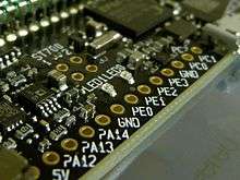
A row of through-holes acting as the footprint for a pin header.
A footprint or land pattern is the arrangement of pads (in surface-mount technology) or through-holes (in through-hole technology) used to physically attach and electrically connect a component to a printed circuit board.[1] The land pattern on a circuit board matches the arrangement of leads on a component.
Component manufacturers often produce multiple pin-compatible product variants to allow systems integrators to change the exact component in use without changing the footprint on the circuit board. This can provide large cost savings for integrators, especially with dense BGA components where the footprint pads may be connected to multiple layers of the circuit board.
See also
- Surface-mount technology
- Through-hole technology
- Chip carrier
- List of integrated circuit packaging types
- IPC (standards body)
- JEDEC (standards body)
References
- ↑ IPC-7351 - Generic Requirements for Surface Mount Design and Land Pattern Standard. IPC. 2005. p. 4.
This article is issued from Wikipedia - version of the 2/12/2016. The text is available under the Creative Commons Attribution/Share Alike but additional terms may apply for the media files.