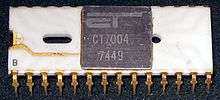
PMOS logic

P-type metal-oxide-semiconductor logic uses p-channel metal-oxide-semiconductor field effect transistors (MOSFETs) to implement logic gates and other digital circuits. PMOS transistors operate by creating an inversion layer in an n-type transistor body. This inversion layer, called the p-channel, can conduct holes between p-type "source" and "drain" terminals.
The p-channel is created by applying voltage to the third terminal, called the gate. Like other MOSFETs, PMOS transistors have four modes of operation: cut-off (or subthreshold), triode, saturation (sometimes called active), and velocity saturation.
The p-type MOSFETs are arranged in a so-called "pull-up network" (PUN) between the logic gate output and positive supply voltage, while a resistor is placed between the logic gate output and the negative supply voltage. The circuit is designed such that if the desired output is high, then the PUN will be active, creating a current path between the positive supply and the output.
While PMOS logic is easy to design and manufacture (a MOSFET can be made to operate as a resistor, so the whole circuit can be made with PMOS FETs), it has several shortcomings as well. The worst problem is that there is a direct current (DC) through a PMOS logic gate when the PUN is active, that is, whenever the output is high, which leads to static power dissipation even when the circuit sits idle.
Also, PMOS circuits are slow to transition from high to low. When transitioning from low to high, the transistors provide low resistance, and the capacitive charge at the output accumulates very quickly (similar to charging a capacitor through a very low resistance). But the resistance between the output and the negative supply rail is much greater, so the high-to-low transition takes longer (similar to discharge of a capacitor through a high resistance). Using a resistor of lower value will speed up the process but also increases static power dissipation.
Additionally, the asymmetric input logic levels make PMOS circuits susceptible to noise.[1]
Most P-MOS integrated circuits require a power supply of 17-24 volt DC.[2] The Intel 4004 PMOS microprocessor uses PMOS logic with polysilicon rather than metal gates. Its positive power supply rail is VSS, and the negative supply rail is VDD; the voltage difference between the rails is 15±5% V.[3] The specified input voltage range for a logic high is VSS−1.5 — VSS+0.3; for a logic low the input range should be VDD — VSS−5.5. For its outputs, the logic high range is VSS−0.5 — VSS, and the logic low range is VSS−12 — VSS−6.5.[3]
Though initially easier to manufacture, PMOS logic was later supplanted by NMOS logic using n-channel field-effect transitors. NMOS is faster than PMOS. Modern integrated circuits are CMOS logic, which uses both p-channel and n-channel transistors.
Full scale replica of the PMOS Intel 4004
A fully functional 130x scale replica of the Intel 4004 was built using discrete transistors and put on display in 2006 at the Intel Museum in Santa Clara, California.[4]
References
- ↑ "Microwave Engineering: Concepts and Fundamentals". 2014. p. 629. Retrieved 2016-04-10.
Also, the asymmetric input logic levels make PMOS circuits susceptible to noise.
- ↑ Fairchild (January 1983). "CMOS, the Ideal Logic Family" (PDF). p. 6. Retrieved 2015-07-03.
Most of the more popular P-MOS parts are specified with 17V to 24V power supplies while the maximum power supply voltage for CMOS is 15V.
- 1 2 "Intel 4004 datasheet" (PDF) (published 2010-07-06). 1987. p. 7. Retrieved 2011-07-06.
- ↑ "Intel 4004 -- 45th Anniversary Project". 2015-11-15. Retrieved 2016-04-02.
including fully functional 130x scale replicas of the 4004 built using discrete transistors, museum-durable keyboards and slide switches, and video display electronics.