Successive approximation ADC
A successive approximation ADC is a type of analog-to-digital converter that converts a continuous analog waveform into a discrete digital representation via a binary search through all possible quantization levels before finally converging upon a digital output for each conversion.
Block diagram

Key
- DAC = digital-to-analog converter
- EOC = end of conversion
- SAR = successive approximation register
- S/H = sample and hold circuit
- Vin = input voltage
- Vref = reference voltage
Algorithm
The successive approximation analog-to-digital converter circuit typically consists of four chief subcircuits:
- A sample and hold circuit to acquire the input voltage (Vin).
- An analog voltage comparator that compares Vin to the output of the internal DAC and outputs the result of the comparison to the successive approximation register (SAR).
- A successive approximation register subcircuit designed to supply an approximate digital code of Vin to the internal DAC.
- An internal reference DAC that, for comparison with VREF, supplies the comparator with an analog voltage equal to the digital code output of the SARin.
The successive approximation register is initialized so that the most significant bit (MSB) is equal to a digital 1. This code is fed into the DAC, which then supplies the analog equivalent of this digital code (Vref/2) into the comparator circuit for comparison with the sampled input voltage. If this analog voltage exceeds Vin the comparator causes the SAR to reset this bit; otherwise, the bit is left a 1. Then the next bit is set to 1 and the same test is done, continuing this binary search until every bit in the SAR has been tested. The resulting code is the digital approximation of the sampled input voltage and is finally output by the SAR at the end of the conversion (EOC).
Mathematically, let Vin = xVref, so x in [−1, 1] is the normalized input voltage. The objective is to approximately digitize x to an accuracy of 1/2n. The algorithm proceeds as follows:
- Initial approximation x0 = 0.
- ith approximation xi = xi−1 − s(xi−1 − x)/2i.
where, s(x) is the signum-function (sgn(x)) (+1 for x ≥ 0, −1 for x < 0). It follows using mathematical induction that |xn − x| ≤ 1/2n.
As shown in the above algorithm, a SAR ADC requires:
- An input voltage source Vin.
- A reference voltage source Vref to normalize the input.
- A DAC to convert the ith approximation xi to a voltage.
- A comparator to perform the function s(xi − x) by comparing the DAC's voltage with the input voltage.
- A register to store the output of the comparator and apply xi−1 − s(xi−1 − x)/2i.

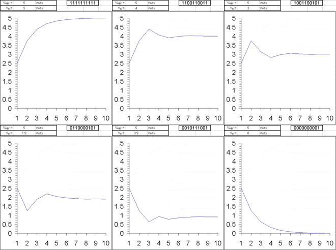
Example: The ten steps to converting an analog input to 10 bit digital, using successive approximation, is shown here, for all voltages from 5V to 0V in 0.1V iterations. Since the reference voltage is 5V, when the input voltage is also 5V all bits are set. As the voltage is decreased to 4.9V, only some of the least significant bits are cleared. The MSB will remain set until the input is one half the reference voltage, 2.5V.
The binary weights assigned to each bit, starting with the MSB, are 2.5, 1.25, 0.625, 0.3125, 0.15625, 0.078125, 0.0390625, 0.01953125, 0.009765625, 0.0048828125. All of these add up to 4.9951171875, meaning binary 1111111111, and is one LSB less than 5.
When the analog input is being compared to the internal DAC output, it effectively is being compared to each of these binary weights, starting with the 2.5V and either keeping it or clearing it as a result. Then by adding the next weight to the previous result, comparing again, and repeating until all the bits and their weights have been compared to the input, the end result, a binary number, representing the analog input, is found.
Charge-redistribution successive approximation ADC

One of the most common implementations of the successive approximation ADC, the charge-redistribution successive approximation ADC, uses a charge scaling DAC. The charge scaling DAC simply consists of an array of individually switched binary-weighted capacitors. The amount of charge upon each capacitor in the array is used to perform the aforementioned binary search in conjunction with a comparator internal to the DAC and the successive approximation register.
- First, the capacitor array is completely discharged to the offset voltage of the comparator, VOS. This step provides automatic offset cancellation(i.e. The offset voltage represents nothing but dead charge which can't be juggled by the capacitors).
- Next, all of the capacitors within the array are switched to the input signal, vIN. The capacitors now have a charge equal to their respective capacitance times the input voltage minus the offset voltage upon each of them.
- In the third step, the capacitors are then switched so that this charge is applied across the comparator's input, creating a comparator input voltage equal to −vIN.
- Finally, the actual conversion process proceeds. First, the MSB capacitor is switched to VREF, which corresponds to the full-scale range of the ADC. Due to the binary-weighting of the array the MSB capacitor forms a 1:1 charge divider with the rest of the array. Thus, the input voltage to the comparator is now −vIN plus VREF/2. Subsequently, if vIN is greater than VREF/2 then the comparator outputs a digital 1 as the MSB, otherwise it outputs a digital 0 as the MSB. Each capacitor is tested in the same manner until the comparator input voltage converges to the offset voltage, or at least as close as possible given the resolution of the DAC.

Use with non-ideal analog circuits
When implemented as an analog circuit – where the value of each successive bit is not perfectly 2N (e.g. 1.1, 2.12, 4.05, 8.01, etc.) – a successive approximation approach might not output the ideal value because the binary search algorithm incorrectly removes what it believes to be half of the values the unknown input cannot be. Depending on the difference between actual and ideal performance, the maximum error can easily exceed several LSBs, especially as the error between the actual and ideal 2N becomes large for one or more bits. Since we don't know the actual unknown input, it is therefore very important that accuracy of the analog circuit used to implement a SAR ADC be very close to the ideal 2N values; otherwise, we cannot guarantee a best match search.
See also
References
- R. J. Baker, CMOS Circuit Design, Layout, and Simulation, Third Edition, Wiley-IEEE, 2010. ISBN 978-0-470-88132-3