Teardrop (electronics)
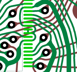
In printed circuit boards, a teardrops are typically drop-shaped features at the junction of vias or contact pads and traces.
The main purpose of teardrops is to enhance structural integrity in presence of thermal or mechanical stresses.[1] Structural integrity may be compromised, e.g., by misalignment during drilling, so that too much copper may be removed by the drill hole in the area where a trace connects to the pad or via.[2] An extra advantage is the enlarging of manufacturing tolerances, making manufacturing easier and cheaper.[3]
While a typical shape of a teardrop is straight-line tapering, they may be concave.[2] To produce a "snowman"-shaped teardrop, a secondary pad of smaller size is added at the junction overlapping with the primary pad (hence the nickname).[4]
References
- ↑ "Component placement tips and strategies", EDN Network
- 1 2 "Enhanced Teardrop Control", Altium Designer technical documentation
- ↑ "Why Where When and how teardrops should be added to PCB? ", Kaizen Technologies
- ↑ "PCB Design Guidelines for 0.5mm Package-on-Package Applications Processor, Part I", Texas Instruments, Application Report SPRABB3, June 2010 (retrieved July 27, 2015)