Thin film
A thin film is a layer of material ranging from fractions of a nanometer (monolayer) to several micrometers in thickness. The controlled synthesis of materials as thin films (a process referred to as deposition) is a fundamental step in many applications. A familiar example is the household mirror, which typically has a thin metal coating on the back of a sheet of glass to form a reflective interface. The process of silvering was once commonly used to produce mirrors, while more recently the metal layer is deposited using techniques such as sputtering. Advances in thin film deposition techniques during the 20th century have enabled a wide range of technological breakthroughs in areas such as magnetic recording media, electronic semiconductor devices, LEDs, optical coatings (such as antireflective coatings), hard coatings on cutting tools, and for both energy generation (e.g. thin film solar cells) and storage (thin-film batteries). It is also being applied to pharmaceuticals, via thin-film drug delivery.
In addition to their applied interest, thin films play an important role in the development and study of materials with new and unique properties. Examples include multiferroic materials, and superlattices that allow the study of quantum confinement by creating two-dimensional electron states.
Deposition
The act of applying a thin film to a surface is thin-film deposition – any technique for depositing a thin film of material onto a substrate or onto previously deposited layers. "Thin" is a relative term, but most deposition techniques control layer thickness within a few tens of nanometres. Molecular beam epitaxy and atomic layer deposition allow a single layer of atoms to be deposited at a time.
It is useful in the manufacture of optics (for reflective, anti-reflective coatings or self-cleaning glass, for instance), electronics (layers of insulators, semiconductors, and conductors form integrated circuits), packaging (i.e., aluminium-coated PET film), and in contemporary art (see the work of Larry Bell). Similar processes are sometimes used where thickness is not important: for instance, the purification of copper by electroplating, and the deposition of silicon and enriched uranium by a CVD-like process after gas-phase processing.
Deposition techniques fall into two broad categories, depending on whether the process is primarily chemical or physical.[1]
Chemical deposition
Here, a fluid precursor undergoes a chemical change at a solid surface, leaving a solid layer. An everyday example is the formation of soot on a cool object when it is placed inside a flame. Since the fluid surrounds the solid object, deposition happens on every surface, with little regard to direction; thin films from chemical deposition techniques tend to be conformal, rather than directional.
Chemical deposition is further categorized by the phase of the precursor:
Plating relies on liquid precursors, often a solution of water with a salt of the metal to be deposited. Some plating processes are driven entirely by reagents in the solution (usually for noble metals), but by far the most commercially important process is electroplating. It was not commonly used in semiconductor processing for many years, but has seen a resurgence with more widespread use of chemical-mechanical polishing techniques.
Chemical solution deposition (CSD) or chemical bath deposition (CBD) uses a liquid precursor, usually a solution of organometallic powders dissolved in an organic solvent. This is a relatively inexpensive, simple thin film process that is able to produce stoichiometrically accurate crystalline phases. This technique is also known as the sol-gel method because the 'sol' (or solution) gradually evolves towards the formation of a gel-like diphasic system.
Spin coating or spin casting, uses a liquid precursor, or sol-gel precursor deposited onto a smooth, flat substrate which is subsequently spun at a high velocity to centrifugally spread the solution over the substrate. The speed at which the solution is spun and the viscosity of the sol determine the ultimate thickness of the deposited film. Repeated depositions can be carried out to increase the thickness of films as desired. Thermal treatment is often carried out in order to crystallize the amorphous spin coated film. Such crystalline films can exhibit certain preferred orientations after crystallization on single crystal substrates.[2]
Dip coating is similar to spin coating in that a liquid precursor or sol-gel precursor is deposited on a substrate, but in this case the substrate is completely submerged in the solution and then withdrawn under controlled conditions. By controlling the withdrawal speed, the evaporation conditions (principally the humidity, temperature) and the volatility/viscosity of the solvent, the film thickness, homogeneity and nanoscopic morphology are controlled. There are two evaporation regimes: the capillary zone at very low withdrawal speeds, and the draining zone at faster evaporation speeds.[3]
Chemical vapor deposition (CVD) generally uses a gas-phase precursor, often a halide or hydride of the element to be deposited. In the case of MOCVD, an organometallic gas is used. Commercial techniques often use very low pressures of precursor gas.
Plasma enhanced CVD (PECVD) uses an ionized vapor, or plasma, as a precursor. Unlike the soot example above, commercial PECVD relies on electromagnetic means (electric current, microwave excitation), rather than a chemical reaction, to produce a plasma.
Atomic layer deposition (ALD) uses gaseous precursor to deposit conformal thin films one layer at a time. The process is split up into two half reactions, run in sequence and repeated for each layer, in order to ensure total layer saturation before beginning the next layer. Therefore, one reactant is deposited first, and then the second reactant is deposited, during which a chemical reaction occurs on the substrate, forming the desired composition. As a result of the stepwise, the process is slower than CVD, however it can be run at low temperatures, unlike CVD.
Physical deposition
Physical deposition uses mechanical, electromechanical or thermodynamic means to produce a thin film of solid. An everyday example is the formation of frost. Since most engineering materials are held together by relatively high energies, and chemical reactions are not used to store these energies, commercial physical deposition systems tend to require a low-pressure vapor environment to function properly; most can be classified as physical vapor deposition (PVD).
The material to be deposited is placed in an energetic, entropic environment, so that particles of material escape its surface. Facing this source is a cooler surface which draws energy from these particles as they arrive, allowing them to form a solid layer. The whole system is kept in a vacuum deposition chamber, to allow the particles to travel as freely as possible. Since particles tend to follow a straight path, films deposited by physical means are commonly directional, rather than conformal.
Examples of physical deposition include: A thermal evaporator that uses an electric resistance heater to melt the material and raise its vapor pressure to a useful range. This is done in a high vacuum, both to allow the vapor to reach the substrate without reacting with or scattering against other gas-phase atoms in the chamber, and reduce the incorporation of impurities from the residual gas in the vacuum chamber. Obviously, only materials with a much higher vapor pressure than the heating element can be deposited without contamination of the film. Molecular beam epitaxy is a particularly sophisticated form of thermal evaporation.
An electron beam evaporator fires a high-energy beam from an electron gun to boil a small spot of material; since the heating is not uniform, lower vapor pressure materials can be deposited. The beam is usually bent through an angle of 270° in order to ensure that the gun filament is not directly exposed to the evaporant flux. Typical deposition rates for electron beam evaporation range from 1 to 10 nanometres per second.
In molecular beam epitaxy (MBE), slow streams of an element can be directed at the substrate, so that material deposits one atomic layer at a time. Compounds such as gallium arsenide are usually deposited by repeatedly applying a layer of one element (i.e., gallium), then a layer of the other (i.e., arsenic), so that the process is chemical, as well as physical. The beam of material can be generated by either physical means (that is, by a furnace) or by a chemical reaction (chemical beam epitaxy).
Sputtering relies on a plasma (usually a noble gas, such as argon) to knock material from a "target" a few atoms at a time. The target can be kept at a relatively low temperature, since the process is not one of evaporation, making this one of the most flexible deposition techniques. It is especially useful for compounds or mixtures, where different components would otherwise tend to evaporate at different rates. Note, sputtering's step coverage is more or less conformal. It is also widely used in the optical media. The manufacturing of all formats of CD, DVD, and BD are done with the help of this technique. It is a fast technique and also it provides a good thickness control. Presently, nitrogen and oxygen gases are also being used in sputtering.
Pulsed laser deposition systems work by an ablation process. Pulses of focused laser light vaporize the surface of the target material and convert it to plasma; this plasma usually reverts to a gas before it reaches the substrate.[4]
Cathodic arc deposition (arc-PVD) which is a kind of ion beam deposition where an electrical arc is created that literally blasts ions from the cathode. The arc has an extremely high power density resulting in a high level of ionization (30–100%), multiply charged ions, neutral particles, clusters and macro-particles (droplets). If a reactive gas is introduced during the evaporation process, dissociation, ionization and excitation can occur during interaction with the ion flux and a compound film will be deposited.
Electrohydrodynamic deposition (electrospray deposition) is a relatively new process of thin film deposition. The liquid to be deposited, either in the form of nano-particle solution or simply a solution, is fed to a small capillary nozzle (usually metallic) which is connected to a high voltage. The substrate on which the film has to be deposited is connected to ground. Through the influence of electric field, the liquid coming out of the nozzle takes a conical shape (Taylor cone) and at the apex of the cone a thin jet emanates which disintegrates into very fine and small positively charged droplets under the influence of Rayleigh charge limit. The droplets keep getting smaller and smaller and ultimately get deposited on the substrate as a uniform thin layer.
Growth modes
Frank-van-der-Merwe[5][6][7] ("layer-by-layer"). In this growth mode the adsorbate-surface and adsorbate-adsorbate interactions are balanced. This type of growth requires lattice matching, and hence considered an "ideal" growth mechanism.
Stranski–Krastanov growth[8] ("joint islands" or "layer-plus-island"). In this growth mode the adsorbate-surface interactions are stronger than adsorbate-adsorbate interactions.
Volmer-Weber[9] ("isolated islands"). In this growth mode the adsorbate-adsorbate interactions are stronger than adsorbate-surface interactions, hence "islands" are formed right away.
Epitaxy
A subset of thin film deposition processes and applications is focused on the so-called epitaxial growth of materials, the deposition of crystalline thin films that grow following the crystalline structure of the substrate. The term epitaxy comes from the Greek roots epi (ἐπί), meaning "above", and taxis (τάξις), meaning "an ordered manner". It can be translated as "arranging upon".
The term homoepitaxy refers to the specific case in which a film of the same material is grown on a crystalline substrate. This technology is used, for instance, to grow a film which is more pure than the substrate, has a lower density of defects, and to fabricate layers having different doping levels. Heteroepitaxy refers to the case in which the film being deposited is different than the substrate.
Techniques used for epitaxial growth of thin films include molecular beam epitaxy, chemical vapor deposition, and pulsed laser deposition.[10]
Thin-film photovoltaic cells
Thin-film technologies are also being developed as a means of substantially reducing the cost of solar cells. The rationale for this is thin film solar cells are cheaper to manufacture owing to their reduced material costs, energy costs, handling costs and capital costs. This is especially represented in the use of printed electronics (roll-to-roll) processes. Other thin-film technologies, that are still in an early stage of ongoing research or with limited commercial availability, are often classified as emerging or third generation photovoltaic cells and include, organic, dye-sensitized, and polymer solar cells, as well as quantum dot, copper zinc tin sulfide, nanocrystal and perovskite solar cells.
Thin-film batteries
Thin-film printing technology is being used to apply solid-state lithium polymers to a variety of substrates to create unique batteries for specialized applications. Thin-film batteries can be deposited directly onto chips or chip packages in any shape or size. Flexible batteries can be made by printing onto plastic, thin metal foil, or paper.[11]
Thin-film Nanocomposites
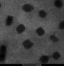
Vertically aligned heteroepitaxial nanocomposite thin films have two phases grown epitaxially on given substrates and form unqiue nanostructures like nanowires in matrix. This kind of nanostructure has very large vertical interfacial area and tunable vertical strain, which can be used to tune functional properties. The STEM image shows a plan-view look of MgO nanowires (dark contrast) grown in La0.7Sr0.3MnO3 thin film matrix (white contrast).[12]
See also
References
- ↑ Functional Polymer Films Eds. R. Advincula and W. Knoll – Wiley, 2011, ISBN 978-3527321902.
- ↑ Hanaor, D; Triani G.; Sorrell C.C.; (2011). "Morphology and photocatalytic activity of highly oriented mixed phase titanium dioxide thin films". Surface and Coatings Technology:. 205 (12): 3658–3664. doi:10.1016/j.surfcoat.2011.01.007.
- ↑ "M. Faustini, G. L. Drisko, C. Boissiere, D. Grosso Liquid deposition approaches to self-assembled periodic nanomasks, Scripta Materiala 2014.". https://www.researchgate.net/publication/256103949_Liquid_deposition_approaches_to_self-assembled_periodic_nanomasks. External link in
|journal=(help) - ↑ Rashidian Vaziri, M R. "Monte Carlo simulation of the subsurface growth mode during pulsed laser deposition". Journal of Applied Physics. 110: 043304. doi:10.1063/1.3624768.
- ↑ Frank, F. C.; van der Merwe, J. H. (1949). "One-Dimensional Dislocations. I. Static Theory". Proceedings of the Royal Society of London. Series A, Mathematical and Physical Sciences. 198 (1053): 205–216. Bibcode:1949RSPSA.198..205F. doi:10.1098/rspa.1949.0095. JSTOR 98165.
- ↑ Frank, F. C.; van der Merwe, J. H. (1949). "One-Dimensional Dislocations. II. Misfitting Monolayers and Oriented Overgrowth". Proceedings of the Royal Society of London. Series A, Mathematical and Physical Sciences. 198 (1053): 216–225. Bibcode:1949RSPSA.198..216F. doi:10.1098/rspa.1949.0096. JSTOR 98166.
- ↑ Frank, F. C.; van der Merwe, J. H. (1949). "One-Dimensional Dislocations. III. Influence of the Second Harmonic Term in the Potential Representation, on the Properties of the Model". Proceedings of the Royal Society of London. Series A, Mathematical and Physical Sciences. 200 (1060): 125–134. Bibcode:1949RSPSA.200..125F. doi:10.1098/rspa.1949.0163. JSTOR 98394.
- ↑ Stranski, I. N.; Krastanov, L. (1938). "Zur Theorie der orientierten Ausscheidung von Ionenkristallen aufeinander". Sitzungsber. Akad. Wiss. Wien. Math.-Naturwiss. 146: 797–810.
- ↑ Volmer, M.; Weber, A. (1926). "Keimbildung in übersättigten Gebilden". Z. Phys. Chem. 119: 277–301.
- ↑ Vaziri, M R R; et al. "Microscopic description of the thermalization process during pulsed laser deposition of aluminium in the presence of argon background gas". Journal of Physics D: Applied Physics. 43: 425205. doi:10.1088/0022-3727/43/42/425205.
- ↑ Flexible Cell Construction. Mpoweruk.com. Retrieved on 2012-01-15.
- ↑ Chen, Aiping; Hu, Jia-Mian; Lu, Ping; Yang, Tiannan; Zhang, Wenrui; Li, Leigang; Ahmed, Towfiq; Enriquez, Erik; Weigand, Marcus; Su, Qing; Wang, Haiyan; Zhu, Jian-Xin; MacManus-Driscoll, Judith L.; Chen, Long-Qing; Yarotski, Dmitry; Jia, Quanxi (2016-06-10). "Role of scaffold network in controlling strain and functionalities of nanocomposite films". Science Advances. 2 (6): e1600245. doi:10.1126/sciadv.1600245. ISSN 2375-2548.
Further reading
Textbooks
- M. Birkholz, with contributions by P.F. Fewster and C. Genzel (2005). Thin Film Analysis by X-Ray Scattering. Weinheim: Wiley-VCH. ISBN 978-3-527-31052-4. Table of contents
- M. Ohring (2001). Materials Science of Thin Films (2nd ed.). Boston: Academic Press. ISBN 9780125249751.
- K. Seshan, ed. (2012). Handbook of Thin Film Deposition (3rd ed.). Amsterdam: Elsevier. ISBN 978-1-4377-7873-1.
Historical
- D.M. Mattox (2003). The Foundations of Vacuum Coating Technology (PDF). Norwich: Noyes / William Andrew Publishing. ISBN 0-8155-1495-6.