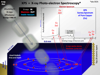
X-ray photoelectron spectroscopy
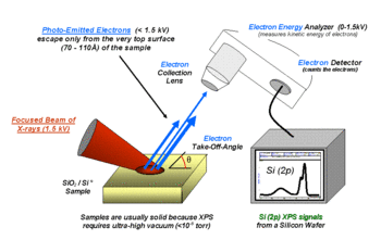
X-ray photoelectron spectroscopy (XPS) is a surface-sensitive quantitative spectroscopic technique that measures the elemental composition at the parts per thousand range, empirical formula, chemical state and electronic state of the elements that exist within a material. XPS spectra are obtained by irradiating a material with a beam of X-rays while simultaneously measuring the kinetic energy and number of electrons that escape from the top 0 to 10 nm of the material being analyzed. XPS requires high vacuum (P ~ 10−8 millibar) or ultra-high vacuum (UHV; P < 10−9 millibar) conditions, although a current area of development is ambient-pressure XPS, in which samples are analyzed at pressures of a few tens of millibar.
XPS can be used to analyze the surface chemistry of a material in its as-received state, or after some treatment, for example: fracturing, cutting or scraping in air or UHV to expose the bulk chemistry, ion beam etching to clean off some or all of the surface contamination (with mild ion etching) or to intentionally expose deeper layers of the sample (with more extensive ion etching) in depth-profiling XPS, exposure to heat to study the changes due to heating, exposure to reactive gases or solutions, exposure to ion beam implant, exposure to ultraviolet light.
- XPS is also known as ESCA (Electron Spectroscopy for Chemical Analysis), an abbreviation introduced by Kai Siegbahn's research group to emphasize the chemical (rather than merely elemental) information that the technique provides.
- In principle XPS detects all elements. In practice, using typical laboratory-scale X-ray sources, XPS detects all elements with an atomic number (Z) of 3 (lithium) and above. It cannot easily detect hydrogen (Z = 1) or helium (Z = 2).
- Detection limits for most of the elements (on a modern instrument) are in the parts per thousand range. Detection limits of parts per million (ppm) are possible, but require special conditions: concentration at top surface or very long collection time (overnight).
- XPS is routinely used to analyze inorganic compounds, metal alloys, semiconductors, polymers, elements, catalysts, glasses, ceramics, paints, papers, inks, woods, plant parts, make-up, teeth, bones, medical implants, bio-materials, viscous oils, glues, ion-modified materials and many others.
- XPS is less routinely used to analyze the hydrated forms of some of the above materials by freezing the samples in their hydrated state in an ultra pure environment, and allowing or causing multilayers of ice to sublime away prior to analysis. Such hydrated XPS analysis allows hydrated sample structures, which may be different from vacuum-dehydrated sample structures, to be studied in their more relevant as-used hydrated structure. Many biomaterials such as hydrogels are examples of such samples.
Measurements
XPS is used to measure:
- elemental composition of the surface (top 0 –10 nm usually)
- empirical formula of pure materials
- elements that contaminate a surface
- chemical or electronic state of each element in the surface
- uniformity of elemental composition across the top surface (or line profiling or mapping)
- uniformity of elemental composition as a function of ion beam etching (or depth profiling)
XPS can be performed using a commercially built XPS system, a privately built XPS system, or a synchrotron-based light source combined with a custom-designed electron energy analyzer. Commercial XPS instruments in the year 2005 used either a focused 20- to 500-micrometer-diameter beam of monochromatic Al Kα X-rays, or a broad 10- to 30-mm-diameter beam of non-monochromatic (polychromatic) Al Kα X-rays or Mg Kα X-rays. A few specially designed XPS instruments can analyze volatile liquids or gases, or materials at pressures of roughly 1 torr (1.00 torr = 1.33 millibar), but there are relatively few of these types of XPS systems. The ability to heat or cool the sample during or prior to analysis is relatively common.
Because the energy of an X-ray with particular wavelength is known (for Al Kα X-rays, Ephoton = 1486.7 eV), and because the emitted electrons' kinetic energies are measured, the electron binding energy of each of the emitted electrons can be determined by using an equation that is based on the work of Ernest Rutherford (1914):

where Ebinding is the binding energy (BE) of the electron, Ephoton is the energy of the X-ray photons being used, Ekinetic is the kinetic energy of the electron as measured by the instrument and is the work function dependent on both the spectrometer and the material. This equation is essentially a conservation of energy equation. The work function term is an adjustable instrumental correction factor that accounts for the few eV of kinetic energy given up by the photoelectron as it becomes absorbed by the instrument's detector. It is a constant that rarely needs to be adjusted in practice.

History
In 1887, Heinrich Rudolf Hertz discovered but could not explain the photoelectric effect, which was later explained in 1905 by Albert Einstein (Nobel Prize in Physics 1921). Two years after Einstein's publication, in 1907, P.D. Innes experimented with a Röntgen tube, Helmholtz coils, a magnetic field hemisphere (an electron kinetic energy analyzer), and photographic plates, to record broad bands of emitted electrons as a function of velocity, in effect recording the first XPS spectrum. Other researchers, including Henry Moseley, Rawlinson and Robinson, independently performed various experiments to sort out the details in the broad bands.
After WWII, Kai Siegbahn and his research group in Uppsala (Sweden) developed several significant improvements in the equipment, and in 1954 recorded the first high-energy-resolution XPS spectrum of cleaved sodium chloride (NaCl), revealing the potential of XPS.[1] A few years later in 1967, Siegbahn published a comprehensive study of XPS, bringing instant recognition of the utility of XPS, which he referred to as ESCA (Electron Spectroscopy for Chemical Analysis). In cooperation with Siegbahn, a small group of engineers (Mike Kelly, Charles Bryson, Lavier Faye, Robert Chaney) at Hewlett-Packard in the USA, produced the first commercial monochromatic XPS instrument in 1969. Siegbahn received the Nobel Prize for Physics in 1981, to acknowledge his extensive efforts to develop XPS into a useful analytical tool.[2]
In parallel with Siegbahn's work, David Turner at Imperial College (and later at Oxford University) in the UK developed ultraviolet photoelectron spectroscopy (UPS) on molecular species using helium lamps.[3]
Basic physics
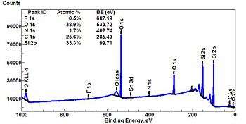
A typical XPS spectrum is a plot of the number of electrons detected (sometimes per unit time) (Y-axis, ordinate) versus the binding energy of the electrons detected (X-axis, abscissa). Each element produces a characteristic set of XPS peaks at characteristic binding energy values that directly identify each element that exists in or on the surface of the material being analyzed. These characteristic spectral peaks correspond to the electron configuration of the electrons within the atoms, e.g., 1s, 2s, 2p, 3s, etc. The number of detected electrons in each of the characteristic peaks is directly related to the amount of element within the XPS sampling volume. To generate atomic percentage values, each raw XPS signal must be corrected by dividing its signal intensity (number of electrons detected) by a "relative sensitivity factor" (RSF), and normalized over all of the elements detected. Since hydrogen is not detected, these atomic percentages exclude hydrogen.
To count the number of electrons during the acquisition of a spectrum with a minimum of error, XPS detectors must be operated under ultra-high vacuum (UHV) conditions because electron counting detectors in XPS instruments are typically one meter away from the material irradiated with X-rays. This long path length for detection requires such low pressures.
Surface sensitivity
XPS detects only those electrons that have actually escaped from the sample into the vacuum of the instrument, and reach the detector. In order to escape from the sample into vacuum, a photoelectron must travel through the sample. Photo-emitted electrons can undergo inelastic collisions, recombination, excitation of the sample, recapture or trapping in various excited states within the material, all of which can reduce the number of escaping photoelectrons. These effects appear as an exponential attenuation function as the depth increases, making the signals detected from analytes at the surface much stronger than the signals detected from analytes deeper below the sample surface. Thus, the signal measured by XPS is an exponentially surface-weighted signal, and this fact can be used to estimate analyte depths in layered materials.
Components of a commercial system

The main components of a commercially made XPS system include a source of X-rays, an ultra-high vacuum (UHV) stainless steel chamber with UHV pumps, an electron collection lens, an electron energy analyzer, Mu-metal magnetic field shielding, an electron detector system, a moderate vacuum sample introduction chamber, sample mounts, a sample stage, and a set of stage manipulators.
Monochromatic aluminium K-alpha X-rays are normally produced by diffracting and focusing a beam of non-monochromatic X-rays off of a thin disc of natural, crystalline quartz with a <1010> orientation. The resulting wavelength is 8.3386 angstroms (0.83386 nm) which corresponds to a photon energy of 1,486.7 eV. Aluminum K-alpha X-rays have an intrinsic FWHM of 0.43 eV, centered on 1,486.7 eV (E/ΔE = 3,457). For a well optimized monochromator, the energy width of the monochromated aluminum K-alpha X-rays is 0.16 eV, but energy broadening in common electron energy analyzers (spectrometers) produces an ultimate energy resolution on the order of FWHM=0.25 eV which, in effect, is the ultimate energy resolution of most commercial systems. When working under practical, everyday conditions, high-energy-resolution settings will produce peak widths (FWHM) between 0.4–0.6 eV for various pure elements and some compounds. For example, in a spectrum obtained in 1 minute at a pass energy of 20 eV using monochromated aluminum K-alpha X-rays, the Ag 3d5/2 peak for a clean silver film or foil will typically have a FWHM of 0.45 eV.
Non-monochromatic magnesium X-rays have a wavelength of 9.89 angstroms (0.989 nm) which corresponds to a photon energy of 1253 eV. The energy width of the non-monochromated X-ray is roughly 0.70 eV, which, in effect is the ultimate energy resolution of a system using non-monochromatic X-rays. Non-monochromatic X-ray sources do not use any crystals to diffract the X-rays which allows all primary X-rays lines and the full range of high-energy Bremsstrahlung X-rays (1–12 keV) to reach the surface. The ultimate energy resolution (FWHM) when using a non-monochromatic Mg K-alpha source is 0.9–1.0 eV, which includes some contribution from spectrometer-induced broadening.
Uses and capabilities
XPS is routinely used to determine:
- What elements and the quantity of those elements that are present within the top 1-12 nm of the sample surface
- What contamination, if any, exists on the surface or in the bulk of the sample
- Empirical formula of a material that is free of excessive surface contamination
- The chemical state identification of one or more of the elements in the sample and also give information on local bonding of atoms
- The binding energy of one or more electronic states
- The thickness of one or more thin layers (1–8 nm) of different materials within the top 12 nm of the surface
- The density of electronic states
Capabilities of advanced systems
- Measure uniformity of elemental composition across the top of the surface (or line profiling or mapping)
- Measure uniformity of elemental composition as a function of depth by ion beam etching (or depth profiling)
- Measure uniformity of elemental composition as a function of depth by tilting the sample (or angle-resolved XPS)
Chemical states and chemical shift
The ability to produce chemical state information (as distinguished from merely elemental information) from the topmost few nm of any surface makes XPS a unique and valuable tool for understanding the chemistry of any surface, either as received, or after physical or chemical treatment(s). In this context, "chemical state" refers to the local bonding environment of a species in question. The local bonding environment of a species in question is affected by its formal oxidation state, the identity of its nearest-neighbor atom, its bonding hybridization to that nearest-neighbor atom, and in some cases even the bonding hybridization between the atom in question and the next-nearest-neighbor atom. Thus, while the nominal binding energy of the C 1s electron is 284.6 eV (some also use 285.0 eV as the nominal value for the binding energy of carbon), subtle but reproducible shifts in the actual binding energy, the so-called chemical shift, provide the chemical state information referred to here.
Chemical-state analysis is widely used for the element carbon. Chemical-state analysis of the surface of carbon-containing polymers readily reveals the presence or absence of the chemical states of carbon shown in bold, in approximate order of increasing binding energy, as: carbide (-C2−), silicone (-Si-CH3), methylene/methyl/hydrocarbon (-CH2-CH2-, CH3-CH2-, and -CH=CH-), amine (-CH2-NH2), alcohol (-C-OH), ketone (-C=O), organic ester (-COOR), carbonate (-CO32−), monofluoro-hydrocarbon (-CFH-CH2-), difluoro-hydrocarbon (-CF2-CH2-), and trifluorocarbon (-CH2-CF3), to name but a few examples.
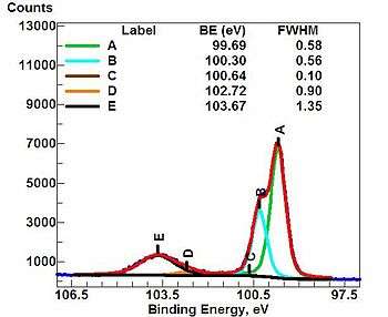
Chemical state analysis of the surface of a silicon wafer readily reveals chemical shifts due to the presence or absence of the chemical states of silicon in its different formal oxidation states, such as: n-doped silicon and p-doped silicon (metallic silicon in figure above), silicon suboxide (Si2O), silicon monoxide (SiO), Si2O3, and silicon dioxide (SiO2). An example of this is seen in the figure above: High-resolution spectrum of an oxidized silicon wafer in the energy range of the Si 2p signal.
Industrial use
- Adhesion
- Agriculture
- Automotive
- Battery
- Biomaterials
- Biomedical
- Biotechnology
- Canning
- Catalyst
- Ceramic
- Chemical
- Computer
- Cosmetics
- Electronics
- Energy
- Environmental
- Fabrics
- Food
- Fuel cells
- Geology
- Glass
- Laser
- Lighting
- Lubrication
- Magnetic storage
- Mineralogy
- Mining
- Nanotechnology
- Nuclear
- Packaging
- Painting
- Paper and wood
- Plating
- Polymer and plastic
- Printing
- Recording
- Semiconductor
- Steel
- Textiles
- Thin-film coating
- Welding
Routine limits
Quantitative accuracy and precision
- XPS is widely used to generate an empirical formula because it readily yields excellent quantitative accuracy from homogeneous solid-state materials.
- Quantification can be divided into two categories: absolute quantification and relative quantification. The former generally requires the use of certified (or independently verified) standard samples, is generally more challenging, and is generally less common.
- Relative quantification is more common and involves comparisons between several samples in a set for which one or more analytes are varied while all other components (the sample matrix) are held constant.
- Quantitative accuracy depends on several parameters such as: signal-to-noise ratio, peak intensity, accuracy of relative sensitivity factors, correction for electron transmission function, surface volume homogeneity, correction for energy dependence of electron mean free path, and degree of sample degradation due to analysis.
- Under optimum conditions, the quantitative accuracy of the atomic percent (at%) values calculated from the Major XPS Peaks is 90-95% for each major peak. If a high level quality control protocol is used, the accuracy can be further improved.
- Under routine work conditions, where the surface is a mixture of contamination and expected material, the accuracy ranges from 80-90% of the value reported in atomic percent values.
- The quantitative accuracy for the weaker XPS signals, that have peak intensities 10-20% of the strongest signal, are 60-80% of the true value, and depend upon the amount of effort used to improve the signal-to-noise ratio (for example by signal averaging).
- Quantitative precision (the ability to repeat a measurement and obtain the same result) is an essential consideration for proper reporting of quantitative results. Standard statistical tests, such as the Student's t test for comparison of means, should be used to determine confidence levels in the average value from a set of replicate measurements, and when comparing the average values of two or more different sets of results. In general, a p value (an output of the Student's t test) of 0.05 or less indicates a level of confidence (95%) that is accepted in the field as significant.
Analysis time
- Typically ranging 1–20 minutes for a broad survey scan that measures the amount of all detectable elements, typically 1–15 minutes for high resolution scan that reveal chemical state differences (for a high signal/noise ratio for count area result often requires multiple sweeps of the region of interest), 1–4 hours for a depth profile that measures 4–5 elements as a function of etched depth (this process time can vary the most as many factors will play a role).
Detection limits
- 0.1–1.0 at% (0.1 at% = 1 part per thousand = 1000 ppm). (Ultimate detection limit for most elements is approximately 100 ppm, which requires 10–16 hours.)
Measured area
- Measured area depends on instrument design. The minimum analysis area ranges from 10 to 200 micrometres. Largest size for a monochromatic beam of X-rays is 1–5 mm. Non-monochromatic beams are 10–50 mm in diameter. Spectroscopic image resolution levels of 200 nm or below has been achieved on latest imaging XPS instruments using synchrotron radiation as X-ray source.
Sample size limits
Instruments accept small (mm range) and large samples (cm range), e.g. wafers. Limiting factor is the design of the sample holder, the sample transfer, and the size of the vacuum chamber. Large samples are laterally moved in x and y direction to analyse a larger area.
Degradation during analysis
- Depends on the sensitivity of the material to the wavelength of X-rays used, the total dose of the X-rays, the temperature of the surface and the level of the vacuum. Metals, alloys, ceramics and most glasses are not measurably degraded by either non-monochromatic or monochromatic X-rays. Some, but not all, polymers, catalysts, certain highly oxygenated compounds, various inorganic compounds and fine organics are degraded by either monochromatic or non-monochromatic X-ray sources.
- Non-monochromatic X-ray sources produce a significant amount of high energy Bremsstrahlung X-rays (1–15 keV of energy) which directly degrade the surface chemistry of various materials. Non-monochromatic X-ray sources also produce a significant amount of heat (100 to 200 °C) on the surface of the sample because the anode that produces the X-rays is typically only 1 to 5 cm (2 in) away from the sample. This level of heat, when combined with the Bremsstrahlung X-rays, acts synergistically to increase the amount and rate of degradation for certain materials. Monochromatic X-ray sources, because they are far away (50–100 cm) from the sample, do not produce any heat effects.
- Monochromatic X-ray sources are monochromatic because the quartz monochromator system diffracts the Bremsstrahlung X-rays out of the X-ray beam, which means the sample is only exposed to one narrow band of X-ray energy. For example, if aluminum K-alpha X-rays are used, the intrinsic energy band has a FWHM of 0.43 eV, centered on 1,486.7 eV (E/ΔE = 3,457). If magnesium K-alpha X-rays are used, the intrinsic energy band has a FWHM of 0.36 eV, centered on 1,253.7 eV (E/ΔE = 3,483). These are the intrinsic X-ray line widths; the range of energies to which the sample is exposed depends on the quality and optimization of the X-ray monochromator.
- Because the vacuum removes various gases (e.g., O2, CO) and liquids (e.g., water, alcohol, solvents, etc.) that were initially trapped within or on the surface of the sample, the chemistry and morphology of the surface will continue to change until the surface achieves a steady state. This type of degradation is sometimes difficult to detect.
General summary of use
- XPS is, in effect, a non-destructive technique that measures the surface chemistry of most any material, however non-dry, outgassing, radioactive or highly magnetic materials can pose serious challenges.
Materials routinely analyzed
Inorganic compounds, metal alloys, semiconductors, polymers, pure elements, catalysts, glasses, ceramics, paints, papers, inks, woods, plant parts, make-up, teeth, bones, human implants, biomaterials,[4] viscous oils, glues, ion modified materials
Analysis details
Charge compensation techniques
- Low-voltage electron beam (1-20 eV) (or electron flood gun)
- UV lights
- Low-voltage argon ion beam with low-voltage electron beam (1-10 eV)
- Aperture masks
- Mesh screen with low-voltage electron beams
Sample preparation
- Sample handling
- Sample cleaning
- Sample mounting
- sample grinding
Data processing
Peak identification
The number of peaks produced by a single element varies from 1 to more than 20. Tables of binding energies (BEs) that identify the shell and spin-orbit of each peak produced by a given element are included with modern XPS instruments, and can be found in various handbooks [citations] and websites.[5] Because these experimentally determined BEs are characteristic of specific elements, they can be directly used to identify experimentally measured peaks of a material with unknown elemental composition.
Before beginning the process of peak identification, the analyst must determine if the BEs of the unprocessed survey spectrum (0-1400 eV) have or have not been shifted due to a positive or negative surface charge. This is most often done by looking for two peaks that due to the presence of carbon and oxygen. {tbc}
Charge referencing insulators
Charge referencing is needed when a sample suffers either a positive (+) or negative (-) charge induced shift of experimental BEs. Charge referencing is needed to obtain meaningful BEs from both wide-scan, high sensitivity (low energy resolution) survey spectra (0-1100 eV), and also narrow-scan, chemical state (high energy resolution) spectra.
Charge induced shifting causes experimentally measured BEs of XPS peaks to appear at BEs that are greater or smaller than true BEs. Charge referencing is performed by adding or subtracting a "Charge Correction Factor" to each of the experimentally measured BEs. In general, the BE of the hydrocarbon peak of the C (1s) XPS signal is used to charge reference (charge correct) all BEs obtained from non-conductive (insulating) samples or conductors that have been deliberately insulated from the sample mount.
Charge induced shifting is normally due to: a modest excess of low voltage (-1 to -20 eV) electrons attached to the surface, or a modest shortage of electrons (+1 to +15 eV) within the top 1-12 nm of the sample caused by the loss of photo-emitted electrons. The degree of charging depends on various factors. If, by chance, the charging of the surface is excessively positive, then the spectrum might appear as a series of rolling hills, not sharp peaks as shown in the example spectrum.
The C (1s) BE of the hydrocarbon species (moieties) of the "Adventitious" carbon that appears on all, air-exposed, conductive and semi-conductive materials is normally found between 284.5 eV and 285.5 eV. For convenience, the C (1s) of hydrocarbon moieties is defined to appear between 284.6 eV and 285.0 eV. A value of 284.8 eV has become popular in recent years. However, some recent reports indicate that 284.9 eV or 285.0 eV represents hydrocarbons attached on metals, not the natural native oxide. The 284.8 eV BE is routinely used as the "Reference BE" for charge referencing insulators. When the C (1s) BE is used for charge referencing, then the charge correction factor is the difference between 284.8 eV and the experimentally measured C (1s) BE of the hydrocarbon moieties.
When using a monochromatic XPS system together with a low voltage electron flood gun for charge compensation the experimental BEs of the C (1s) hydrocarbon peak is often 4-5 eV smaller than the reference BE value (284.8 eV). In this case, all experimental BEs appear at lower BEs than expected and need to be increased by adding a value ranging from 4 to 5 eV. Non-monochromatic XPS systems are not usually equipped with a low voltage electron flood gun so the BEs will normally appear at higher BEs than expected. It is normal to subtract a charge correction factor from all BEs produced by a non-monochromatic XPS system.
Conductive materials and most native oxides of conductors should never need charge referencing. Conductive materials should never be charge referenced unless the topmost layer of the sample has a thick non-conductive film.
Peak-fitting
The process of peak-fitting high energy resolution XPS spectra is still a mixture of art, science, knowledge and experience. The peak-fit process is affected by instrument design, instrument components, experimental settings (aka analysis conditions) and sample variables. Most instrument parameters are constant while others depend on the choice of experimental settings.
Before starting any peak-fit effort, the analyst performing the peak-fit needs to know if the topmost 15 nm of the sample is expected to be a homogeneous material or is expected to be a mixture of materials. If the top 15 nm is a homogeneous material with only very minor amounts of adventitious carbon and adsorbed gases, then the analyst can use theoretical peak area ratios to enhance the peak-fitting process.
Variables that affect or define peak-fit results include:
- FWHMs
- Chemical Shifts
- Peakshapes
- Instrument design factors
- Experimental settings
- Sample factors
FWHMs
- When using high energy resolution experiment settings on an XPS equipped with a monochromatic Al K-alpha X-ray source, the FWHM of the major XPS peaks range from 0.3 eV to 1.7 eV. The following is a simple summary of FWHM from major XPS signals:
- Main metal peaks (e.g. 1s, 2p3, 3d5, 4f7) from pure metals have FWHMs that range from 0.30 eV to 1.0 eV
- Main metal peaks (e.g. 1s, 2p3, 3d5, 4f7) from binary metal oxides have FWHMs that range from 0.9 eV to 1.7 eV
- The O (1s) peak from binary metal oxides have FWHMs that, in general, range from 1.0 eV to 1.4 eV
- The C (1s) peak from adventitious hydrocarbons have FWHMs that, in general, range from 1.0 eV to 1.4 eV
However, it should be noted that the FWHM also depends on the detector, and can also increase due to the sample getting charged.
Chemical shifts
Chemical shift values depend on the degree of electron bond polarization between nearest neighbor atoms. A specific chemical shift is the difference in BE values of one specific chemical state versus the BE of one form of the pure element, or of a particular agreed-upon chemical state of that element. Component peaks derived from peak-fitting a raw chemical state spectrum can be assigned to the presence of different chemical states within the sampling volume of the sample.
Peak shapes
- Depends on instrument parameters, experimental parameters and sample characteristics
Instrument design factors
- FWHM and purity of X-rays used (monochromatic Al, non-monochromatic Mg, Synchrotron, Ag, Zr...)
- Design of electron analyzer (CMA, HSA, retarding field...)
Experiment settings
- Settings of the electron analyzer (e.g. pass energy, step size)
Sample factors
- Physical form of the sample (single crystal, polished, powder, corroded...)
- Number of physical defects within the analysis volume (from Argon ion etching, from laser cleaning...)
Advanced instrumentation aspects
Hemispherical electron energy analyzer
A hemispherical electron energy analyser is generally used for applications where a higher resolution is needed. An ideal hemispherical analyser consists of two concentric hemispherical electrodes (inner and outer hemispheres) held at proper voltages. It is possible to demonstrate that in such a system, (i) the electrons are linearly dispersed along the direction connecting the entrance and the exit slit, depending on their kinetic energy, while (ii) electrons with the same energy are first-order focused.[6] When two potentials, and , are applied to the inner and outer hemispheres, respectively, the electric potential and field in the region between the two electrodes can be calculated by solving the Laplace equation:


![V(r)=-\left[{\frac {(V_{{2}}-V_{{1}})}{(R_{{2}}-R_{{1}})}}\right]\cdot {\frac {(R_{{1}}R_{{2}})}{r}}+const.](../I/m/7253e059f42abfe021558aa06a893fa9047d0abc.svg)
![|E(r)|=-\left[{\frac {(V_{{2}}-V_{{1}})}{(R_{{2}}-R_{{1}})}}\right]\cdot {\frac {(R_{{1}}R_{{2}})}{r^{{2}}}}](../I/m/75010d0e9e9852186e163276b2699841d3ae632c.svg)
where and are the radii of the two hemispheres. In order for the electrons with kinetic energy E0 to follow a circular trajectory of radius , the force exerted by the electric field () must equal the centripetal force () along the whole path. After some algebra, the following expression can be derived for the potential:


- ,

where is the energy of the electrons expressed in eV. From this equation, we can calculate the potential difference between the two hemispheres, which is given by:

- .

The latter equation can be used to determine the potentials to be applied to the hemispheres in order to select electrons with energy , the so-called pass energy.

In fact, only the electrons with energy impinging normal to the entrance slit of the analyzer describe a trajectory of radius and reach the exit slit, where they are revealed by the detector.


The instrumental energy resolution of the device depends both on the geometrical parameters of the analyzer and on the angular divergence of the incoming photoelectrons:
- ,

where is the average width of the two slits, and is the incidence angle of the incoming photoelectrons. Though the resolution improves with increasing , technical problems related to the size of the analyser put a limit on the actual value of . Although a low pass energy improves the resolution, the electron transmission probability is reduced at low pass energy, and the signal-to-noise ratio deteriorates, accordingly. The electrostatic lenses in front of the analyser have two main purposes: they collect and focus the incoming photoelectrons into the entrance slit of the analyzer, and they decelerate the electrons to the kinetic energy , in order to increase the resolution.


When acquiring spectra in sweep (or scanning) mode, the voltages of the two hemispheres and - and hence the pass energy- are held fixed; at the same time, the voltage applied to the electrostatic lenses is swept in such a way that each channel counts electrons with the selected kinetic energy for the selected amount of time. In order to reduce the acquisition time per spectrum, the so-called snapshot (or fixed) mode has been introduced. This mode exploits the relation between the kinetic energy of a photoelectron and its position inside the detector. If the detector energy range is wide enough, and if the photoemission signal collected from all the channels is sufficiently strong, the photoemission spectrum can be obtained in one single shot from the image of the detector.
Cylindrical mirror analyser
Since the relevant information, in photoemission spectroscopy, is contained in the kinetic energy distribution of the photoelectrons, a specific device is needed to energy-filter the electrons emitted (or scattered) by the sample. Electrostatic monochromators are the most common choice. The older design, a CMA, represents a trade-off between the need for high count rates and high angular/energy resolution. The so-called cylindrical mirror analyser (CMA) is mostly used for checking the elemental composition of the surface. It consists of two co-axial cylinders placed in front of the sample, the inner one being held at a positive potential, while the outer cylinder is held at a negative potential. Only the electrons with the right energy can pass through this set-up and are detected at the end. The count rates are high but the resolution (both in energy and angle) is poor.
Synchrotron based XPS
A breakthrough has been actually brought about in the last decades by the development of large scale synchrotron radiation facilities. Here, bunches of relativistic electrons kept on a circular orbit inside a storage ring are accelerated through bending magnets or insertion devices like wigglers and undulators to produce a high brilliance and high flux photon beam. The main advantages of using synchrotron light are
- the high brilliance of this kind of radiation, which is orders of magnitude more intense and better collimated than the one produced by anode-based sources;
- the tunability of synchrotron radiation over a wide frequency range;
- its high polarization;
- the high photon flux;
- the possibility of producing extremely short pulses at a frequency as high as a MHz.
The highest spectral brightness and narrowest beam energy dispersion is attained by undulators, which consist of periodic array of dipole magnets in which the electrons are forced to wiggle and thus to emit coherent light. Besides the high intensity, energy tunability is one of the most important advantages of synchrotron light compared to the light produced by conventional X-ray sources. In fact, a wide energy range (from the IR to the Hard X-ray region, depending on the energy of the electron bunch) is accessible by changing the undulator gaps between the arrays. Continuous energy spectra available from a synchrotron radiation source allows selection of photon energies yielding optimum photoionization cross-sections appropriate for probing a particular core level. The high photon flux, in addition, makes it possible to perform XPS experiments also from low density atomic species, such as molecular and atomic adsorbates.
Electron detectors
Older style electron detector
Electrons can be detected using an electron multiplier, usually a channeltron. This device essentially consists of a glass tub with a resistive coating on the inside. A high voltage is applied between the front and the end. An electron which enters the channeltron is accelerated to the wall, where it removes more electrons, in such a way that an electron avalanche is created, until a measurable current pulse is obtained.
Theoretical aspects
Quantum mechanical treatment
When a photoemission event takes place, the following energy conservation rule holds:

where is the photon energy, is the electron BE (with respect to the vacuum level) prior to ionization, and is the kinetic energy of the photoelectron. If reference is taken with respect to the Fermi level (as it is typically done in photoelectron spectroscopy) must be replaced by the sum of the binding energy (BE) relative to the Fermi level, , and the sample work function, .


From the theoretical point of view, the photoemission process from a solid can be described with a semiclassical approach, where the electromagnetic field is still treated classically, while a quantum-mechanical description is used for matter. The one—particle Hamiltonian for an electron subjected to an electromagnetic field is given by:
- ,
![i\hbar {\frac {\partial \psi }{\partial t}}=\left[{\frac {1}{2m}}\left({\mathbf {{\hat {p}}}}-{\frac {e}{c}}{\mathbf {{\hat {A}}}}\right)^{2}+{\hat {V}}\right]\psi ={\hat {H}}\psi](../I/m/c603af3e1e3199055c397049778e6a5b5827f403.svg)
where is the electron wave function, is the vector potential of the electromagnetic field and is the unperturbed potential of the solid. In the Coulomb gauge (), the vector potential commutes with the momentum operator (), so that the expression in brackets in the Hamiltonian simplifies to:


![[{\mathbf {{\hat {p}}}},{\mathbf {{\hat {A}}}}]=0](../I/m/cb8170b2148b65517ad2ca4aa3d2596b581d7502.svg)

Actually, neglecting the term in the Hamiltonian, we are disregarding possible photocurrent contributions.[7] Such effects are generally negligible in the bulk, but may become important at the surface. The quadratic term in can be instead safely neglected, since its contribution in a typical photoemission experiment is about one order of magnitude smaller than that of the first term .

In first-order perturbation approach, the one-electron Hamiltonian can be split into two terms, an unperturbed Hamiltonian , plus an interaction Hamiltonian , which describes the effects of the electromagnetic field:


In the time-dependent perturbation theory for harmonic perturbations, the transition rate between the initial state and the final state is expressed by the Fermi's golden rule:


- ,

where and are the eigenvalues of the unperturbed Hamiltonian in the initial and final state, respectively, and is the photon energy. The Fermi Golden rule strictly applies only if the perturbation acts on the system for an infinite time. Since in a real system the interaction has a finite duration, the Dirac delta function in the equation above must be replaced by the density of states in the final state, :


In a real photoemission experiment the ground state core electron BE cannot be directly probed, because the measured BE incorporates both initial state and final state effects, and the spectral linewidth is broadened owing to the finite core-hole lifetime ().

Assuming an exponential decay probability for the core hole in the time domain (), the spectral function will have a Lorentzian shape, with a FWHM (Full Width at Half Maximum) given by:


From the theory of Fourier transforms, and are linked by the indeterminacy relation:

The photoemission event leaves the atom in a highly excited core ionized state, from which it can decay radiatively (fluorescence) or non-radiatively (typically by Auger decay). Besides Lorentzian broadening, photoemission spectra are also affected by a Gaussian broadening, whose contribution can be expressed by

Three main factors enter the Gaussian broadening of the spectra: the experimental energy resolution, vibrational and inhomogeneous broadening. The first effect is caused by the non perfect monochromaticity of the photon beam -which results in a finite bandwidth- and by the limited resolving power of the analyser. The vibrational component is produced by the excitation of low energy vibrational modes both in the initial and in the final state. Finally, inhomogeneous broadening can originate from the presence of unresolved core level components in the spectrum.
Theory of core level photoemission of electrons
In a solid, also inelastic scattering events contribute to the photoemission process, generating electron-hole pairs which show up as an inelastic tail on the high BE side of the main photoemission peak. In some cases, we observe also energy loss features due to plasmon excitations. This can either a final state effect caused by core hole decay, which generates quantized electron wave excitations in the solid (intrinsic plasmons), or it can be due to excitations induced by photoelectrons travelling from the emitter to the surface (extrinsic plasmons). Due to the reduced coordination number of first-layer atoms, the plasma frequency of bulk and surface atoms are related by the following equation: , so that surface and bulk plasmons can be easily distinguished from each other. Plasmon states in a solid are typically localized at the surface, and can strongly affect the electron Inelastic Mean Free Path (IMFP).

Vibrational effects
Temperature-dependent atomic lattice vibrations, or phonons, can broaden the core level components and attenuate the interference patterns in an XPD (X-Ray Photoelectron Diffraction) experiment. The simplest way to account for vibrational effects is by multiplying the scattered single-photoelectron wave function by the Debye-Waller factor:

- ,

where is the squared magnitude of the wave vector variation caused by scattering, and is the temperature-dependent one-dimensional vibrational mean squared displacement of the emitter. In the Debye model, the mean squared displacement is calculated in terms of the Debye temperature, , as:


See also
- Photoemission spectroscopy
- Ultra-violet photoelectron spectroscopy
- List of materials analysis methods
- Covariance mapping
Related methods
- UPS, Ultra-violet photoelectron spectroscopy
- PES, Photoemission spectroscopy
- ZEKE, Zero Electron Kinetic Energy spectroscopy
- AES, Auger electron spectroscopy
- EDS, energy dispersive X-ray spectroscopy, (EDX or EDXRF)
- PEEM, Photoelectron emission microscopy
References
- ↑ Siegbahn, K.; Edvarson, K. I. Al (1956). "β-Ray spectroscopy in the precision range of 1 : 1e6". Nuclear Physics. 1 (8): 137–159. Bibcode:1956NucPh...1..137S. doi:10.1016/S0029-5582(56)80022-9.
- ↑ Electron Spectroscopy for Atoms, Molecules and Condensed Matter, Nobel Lecture, December 8, 1981
- ↑ Turner, D. W.; Jobory, M. I. Al (1962). "Determination of Ionization Potentials by Photoelectron Energy Measurement". The Journal of Chemical Physics. 37 (12): 3007. Bibcode:1962JChPh..37.3007T. doi:10.1063/1.1733134.
- ↑ Ray, S. and A.G. Shard, Quantitative Analysis of Adsorbed Proteins by X-ray Photoelectron Spectroscopy. Analytical Chemistry, 2011. 83(22): p. 8659-8666.
- ↑ "Handbook of The Elements and Native Oxides" (PDF). XPS International, Inc. Retrieved 8 December 2012.
- ↑ Hadjarab, F.; J.L. Erskine (1985). "Image properties of the hemispherical analyzer applied to multichannel energy detection". Journal of Electron Spectroscopy and related Phenomena. 36 (3): 227. doi:10.1016/0368-2048(85)80021-9.
- ↑ Hüfner, S. (1995). Photoelectron spectroscopy: principles and applications. Springer Verlag.
Further reading
- Handbooks of Monochromatic XPS Spectra - Fully Annotated, PDF of Volumes 1 and 2, B.V.Crist, published by XPS International LLC, 2005, Mountain View, CA, USA
- Handbooks of Monochromatic XPS Spectra, Volumes 1-5, B.V.Crist, published by XPS International LLC, 2004, Mountain View, CA, USA
- Surface Analysis by Auger and X-ray Photoelectron Spectroscopy, ed. J.T.Grant and D.Briggs, published by IM Publications, 2003, Chichester, UK
- An Introduction to Surface Analysis by XPS and AES, J.F.Watts, J.Wolstenholme, published by Wiley & Sons, 2003, Chichester, UK, ISBN 978-0-470-84713-8
- Practical Surface Analysis by Auger and X-ray Photoelectron Spectroscopy, 2nd edition, ed. M.P.Seah and D.Briggs, published by Wiley & Sons, 1992, Chichester, UK
- Practical Surface Analysis by Auger and X-ray Photoelectron Spectroscopy, ed. M.P.Seah and D.Briggs, published by Wiley & Sons, 1983, Chichester, UK ISBN 0-471-26279-X
- Surface Chemical Analysis — Vocabulary, ISO 18115 : 2001, International Organisation for Standardisation (ISO), TC/201, Switzerland,
- Handbook of X-ray Photoelectron Spectroscopy, J.F.Moulder, W.F.Stickle, P.E.Sobol, and K.D.Bomben, published by Perkin-Elmer Corp., 1992, Eden Prairie, MN, USA
External links
- X-Ray Photoelectron Spectroscopy Overview
- The conventional X-Ray source at the Surface Science Laboratory - Instrumental description and guided tour
- The SuperESCA beamline @ Elettra Welcome to the Fast XPS beamline!
- Monochromated XPS Technique background information, useful analysis resources and monochromated XPS equipment description.