ARM9
| Instruction set |
ARM (32-bit), Thumb (16-bit) (alternate). ARM Architecture: ARMv4T |
|---|
| Instruction set |
ARM (32-bit), Thumb (16-bit) (alternate). ARM Architecture:, ARMv5TE |
|---|
| Instruction set |
ARM (32-bit), Thumb (16-bit) (alternate), Jazelle (8-bit) (alternate). ARM Architecture:, ARMv5TEJ |
|---|
ARM9 is a group of older 32-bit RISC ARM processor cores licensed by ARM Holdings.
Overview
With this design generation, ARM moved from a von Neumann architecture (Princeton architecture) to a Harvard architecture with separate instruction and data buses (and caches), significantly increasing its potential speed.[1] Most silicon chips integrating these cores will package them as modified Harvard architecture chips, combining the two address buses on the other side of separated CPU caches and tightly coupled memories.
There are two subfamilies, implementing different ARM architecture versions.
Differences from ARM7 cores
Key improvements over ARM7 cores, enabled by spending more transistors, include:[2]
- Decreased heat production and lower overheating risk.
- Clock frequency improvements. Shifting from a three-stage pipeline to a five-stage one lets the clock speed be approximately doubled, on the same silicon fabrication process.
- Cycle count improvements. Many unmodified ARM7 binaries were measured as taking about 30% fewer cycles to execute on ARM9 cores. Key improvements include:
- Faster loads and stores; many instructions now cost just one cycle. This is helped by both the modified Harvard architecture (reducing bus and cache contention) and the new pipeline stages.
- Exposing pipeline interlocks, enabling compiler optimizations to reduce blockage between stages.
Additionally, some ARM9 cores incorporate "Enhanced DSP" instructions, such as a multiply-accumulate, to support more efficient implementations of digital signal processing algorithms.
Switching to a Harvard architecture entailed a non-unified cache, so that instruction fetches do not evict data (and vice versa). ARM9 cores have separate data and address bus signals, which chip designers use in various ways. In most cases they connect at least part of the address space in von Neumann style, used for both instructions and data, usually to an AHB interconnect connecting to a DRAM interface and an External Bus Interface usable with NOR flash memory. Such hybrids are no longer pure Harvard architecture processors.
Cores
| Year | ARM9 Cores |
|---|---|
| 1998 | ARM9TDMI |
| 1998 | ARM940T |
| 1999 | ARM9E-S |
| 1999 | ARM966E-S |
| 2000 | ARM920T |
| 2000 | ARM922T |
| 2000 | ARM946E-S |
| 2001 | ARM9EJ-S |
| 2001 | ARM926EJ-S |
| 2004 | ARM968E-S |
| 2006 | ARM996HS |
The ARM MPCore family of multicore processors support software written using either the asymmetric (AMP) or symmetric (SMP) multiprocessor programming paradigms. For AMP development, each central processor unit within the MPCore may be viewed as an independent processor and as such can follow traditional single processor development strategies.[3]
ARM9TDMI
ARM9TDMI is a successor to the popular ARM7TDMI core, and is also based on the ARMv4T architecture. Cores based on it support both 32-bit ARM and 16-bit Thumb instruction sets and include:
- ARM920T with 16 KB each of I/D cache and an MMU
- ARM922T with 8 KB each of I/D cache and an MMU
- ARM940T with cache and a Memory Protection Unit (MPU)
ARM9E and ARM9EJ
ARM9E, and its ARM9EJ sibling, implement the basic ARM9TDMI pipeline, but add support for the ARMv5TE architecture, which includes some DSP-esque instruction set extensions. In addition, the multiplier unit width has been doubled, halving the time required for most multiplication operations. They support 32-bit, 16-bit, and sometimes 8-bit instruction sets.
- ARM926EJ-S with ARM Jazelle technology, which enables the direct execution of 8-bit Java bytecode in hardware, and an MMU
- ARM946
- ARM966
- ARM968
Chips


- ASPEED AST2400
- Atmel AT91SAM9, AT91CAP9
- CSR Quatro 4300
- Cirrus Logic EP9315 ARM9 CPU, 200 MHz
- Cypress Semiconductor EZ-USB FX3
- Digi NS9215, NS9210[4]
- Infineon S-GOLDlite PMB 8875
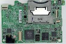
- Nintendo NTR-CPU (Nintendo DS CPU), TWL-CPU (Nintendo DSi CPU; same as the DS but clocked at 132 MHz instead of 66 MHz)
- NXP Semiconductors LPC3200, LPC3100, LPC2900, LH7A
- Freescale Semiconductor i.MX1x and i.MX2x
- Marvell Kirkwood
- Qualcomm MSM6xxx
- Qualcomm Atheros AR6400
- HiSilicon Kirin K3V1
- Samsung S3C24xx
- STMicroelectronics STR9 series,[5] Nomadik
- Texas Instruments OMAP 1
- Texas Instruments Sitara AM1x
- Texas Instruments TMS320DM365/TMS320DM368 ARM9EJ-S
- Via WonderMedia 8505 and 8650
- MediaTek MT6516, MT6573
- Zilog Encore! 32
Documentation
The amount of documentation for all ARM chips is daunting, especially for newcomers. The documentation for microcontrollers from past decades would easily be inclusive in a single document, but as chips have evolved so has the documentation grown. The total documentation is especially hard to grasp for all ARM chips since it consists of documents from the IC manufacturer and documents from CPU core vendor (ARM Holdings).
A typical top-down documentation tree is: high-level marketing slides, datasheet for the exact physical chip, a detailed reference manual that describes common peripherals and other aspects of physical chips within the same series, reference manual for the exact ARM core processor within the chip, reference manual for the ARM architecture of the core which includes detailed description of all instruction sets.
- Documentation tree (top to bottom)
- IC manufacturer marketing slides.
- IC manufacturer datasheets.
- IC manufacturer reference manuals.
- ARM core reference manuals.
- ARM architecture reference manuals.
IC manufacturer has additional documents, including: evaluation board user manuals, application notes, getting started with development software, software library documents, errata, and more.
See also
- ARM architecture
- List of ARM microprocessor cores
- Microcontroller
- List of common microcontrollers
- Embedded system
- Single-board microcontroller
- Interrupt
- Interrupt handler
- Comparison of real-time operating systems
- JTAG
References
- ↑ Furber, Steve. ARM System-on-Chip Architecture. p. 344. ISBN 0201675196.
- ↑ "Performance of the ARM9TDMI and ARM9E-S cores compared to the ARM7TDMI core", Issue 1.0, dated 9 February 2000, ARM Ltd.
- ↑ "MPCore Sample Code". Archived from the original on 11 April 2015.
- ↑ "NS9210/NS9215 32-bit NET+ARM Processor Family" (PDF). Digi International.
- ↑ STR9 Website; STMicroelectronics.
External links
- ARM Holdings
- Quick Reference Cards
- Instructions: Thumb (1), ARM and Thumb-2 (2), Vector Floating Point (3)
- Opcodes: Thumb (1, 2), ARM (3, 4), GNU Assembler Directives 5.
- Yurichev, Dennis, "An Introduction To Reverse Engineering for Beginners" including ARM assembly. Online book: http://yurichev.com/writings/RE_for_beginners-en.pdf