LGA 1155
 | |
| Type | LGA |
|---|---|
| Contacts | 1155 |
| Processor dimensions | 37.5 × 37.5 mm[1] |
| Processors | Sandy Bridge, Ivy Bridge |
| Predecessor | LGA 1156 |
| Successor | LGA 1150 |
|
This article is part of the CPU socket series | |

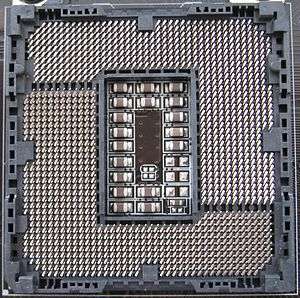
LGA 1155, also called Socket H2, is a socket used for Intel microprocessors based on Sandy Bridge and Ivy Bridge microarchitectures. It was designed as a replacement for LGA 1156 (known as Socket H).
LGA 1155 has 1155 protruding pins to make contact with the pads on the processor. The pins are arranged in a 40×40 array with a 24×16 central void and additional 61 omitted pins (two adjoining the central void, six in each of the four corners, and 35 in groups around the perimeter), yielding the 1600 − 384 − 61 = 1155 pin count. Processors for LGA 1155 and LGA 1156 sockets are not compatible with each other since they have different socket notches. Cooling systems are compatible between LGA 1155 and LGA 1156 sockets, as the processors have the same dimensions, profile and construction, and similar levels of heat production.[2]
Original Sandy Bridge chipsets
Sandy Bridge chipsets, except Q65, Q67 and B65, support both Sandy Bridge and Ivy Bridge CPUs through a BIOS upgrade.[3] Sandy Bridge based processors officially support up to DDR3-1333 memory, however in practice speeds up to DDR3-2133 have been tested to work successfully.[4]
The H61 chipset only supports one double-sided DIMM per memory-channel and therefore is limited to 16 GB instead of the 32 GB like the others support.[5] On H61-based motherboards with four DIMM slots, only four single-sided DIMMs can be installed.[6]
| Name[7] | B65 | H61 | Q67 | H67[8] | P67 | Z68[9] |
|---|---|---|---|---|---|---|
| Overclocking | GPU | CPU + RAM | CPU + GPU + RAM | |||
| Allows using built-in GPU with Intel Clear Video Technology | Yes | No | Yes | |||
| Maximum USB 2.0 ports[lower-alpha 1] | 12 | 10 | 14 | |||
| Maximum SATA 2.0/3.0 ports | 4 / 1 | 4 / 0 | 4 / 2 | |||
| Main PCIe configuration | 1 × PCIe 2.0 ×16 |
| ||||
| Secondary PCIe | 8 × PCIe 2.0 ×1 | 6 × PCIe 2.0 ×1 | 8 × PCIe 2.0 ×1 | |||
| Conventional PCI support[lower-alpha 2] | Yes | No | Yes | No | ||
| Intel Rapid Storage Technology (RAID) | No | Yes | ||||
| Smart Response Technology | No | Yes | ||||
| Ivy Bridge processor support | No | Yes | No | Yes | ||
| Intel Active Management, Trusted Execution, Anti-Theft, and vPro Technology | No | Yes | No | |||
| Release date | February 2011 | May 2011 | January 2011 | May 2011 | ||
| Maximum TDP | 6.1 W | |||||
| Chipset lithography | 65 nm | |||||
Ivy Bridge chipsets
All Ivy Bridge chipsets and motherboards support both Sandy Bridge and Ivy Bridge CPUs. Ivy Bridge based processors will officially support up to DDR3-1600, up from DDR3-1333 of Sandy Bridge. Some consumer Ivy Bridge chipsets will also allow overclocking of K-series processors.[10]
| Name[11] | B75 | Q75 | Q77 | H77 | Z75 | Z77 |
|---|---|---|---|---|---|---|
| Overclocking | CPU (Bclk) + GPU | CPU + GPU + RAM | ||||
| Allows using built-in GPU | Yes | |||||
| Intel Clear Video Technology | Yes | |||||
| RAID | No | Yes | ||||
| Maximum USB 2.0/3.0 ports | 8 / 4 | 10 / 4 | ||||
| Maximum SATA 2.0/3.0 ports | 5 / 1 | 4 / 2 | ||||
| Main PCIe configuration[lower-alpha 3] | 1 × PCIe 3.0 ×16 |
|
| |||
| Secondary PCIe | 8 PCIe 2.0 ×1 | |||||
| Conventional PCI[lower-alpha 2] | Yes | No [12] | ||||
| Intel Rapid Storage Technology | No | Yes | ||||
| Intel Anti-Theft Technology | Yes | |||||
| Smart Response Technology | No | Yes | No | Yes | ||
| Intel vPro | No | Yes | No | |||
| Release date | April 2012[13] | |||||
| Maximum TDP | 6.7 W | |||||
| Chipset lithography | 65 nm[14] | |||||
See also
Notes
- ↑ USB 3.0 is not supported by any of these chipsets. Motherboard manufacturers may use external hardware to add USB 3.0 support.
- 1 2 Although some of the chipsets do not support conventional PCI, motherboard manufacturers may include support through the addition of third-party PCI bridges.
- ↑ For PCIe 3.0 capability, the Ivy Bridge CPU must have the relevant PCIe 3.0 controller built in. However, some Ivy Bridge CPUs only have a PCIe 2.0 controller built in.
References
- ↑ "Intel Core 2 gen CPUs and Socket 1155 Datasheet" (PDF).
- ↑ "2nd Gen Intel Core Processor, LGA1155 Socket:" (PDF). Download.intel.com. Retrieved 2012-09-26.
- ↑ "Ivy Bridge Quad-Core to Have 77W TDP, Intel Plans for LGA1155 Ivy Bridge Entry". techPowerUp. Retrieved 2012-09-26.
- ↑ "Sandy Bridge Memory Scaling: Choosing the Best DDR3". AnandTech. Retrieved 2012-09-26.
- ↑ "Intel H61 Express Chipset". Intel.com. Retrieved 2012-09-26.
- ↑ "Motherboards- ASUS P8H61 EVO". ASUS. Retrieved 2012-09-26.
- ↑ "ARK - Compare Intel Products". Intel ARK (Product Specs).
- ↑ "Intel H67 Express Chipset". Intel.com. Retrieved 2012-09-26.
- ↑ "Intel SSD Caching Feature for Z68 Chipset Explored". Vr-zone.com. 2011-04-25. Retrieved 2012-09-26.
- ↑ "Intel's Roadmap: Ivy Bridge, Panther Point, and SSDs". AnandTech. Retrieved 2012-09-26.
- ↑ "ARK - Compare Intel Products". Intel ARK (Product Specs).
- ↑ "Intel 7 Series Chipset Family PCH: Datasheet". Intel.com. Retrieved 2014-12-02.
- ↑ "Intel 7-Series Chipset Officially Debuts, Derived Desktop Board Products Launched". techPowerUp. Retrieved 2012-09-26.
- ↑ "ARK | Intel Z77 Express Chipset (Intel BD82Z77 PCH)". Ark.intel.com. Retrieved 2012-09-26.