Leo Esaki
| Leo Esaki | |
|---|---|
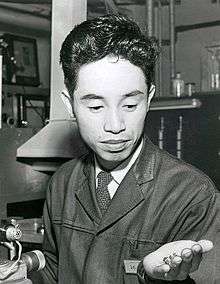
 Leo Esaki in 1959 | |
| Born |
March 12, 1925[1] Osaka, Japan |
| Nationality | Japanese |
| Fields | Applied physics |
| Known for | electron tunneling, Esaki diode |
| Notable awards |
Asahi Prize (1959) Stuart Ballantine Medal (1961) Japan Academy Prize (1965) Nobel Prize in Physics (1973) Harold Pender Award (1989) IEEE Medal of Honor (1991) Japan Prize (1998)[1] |
Reona Esaki (江崎 玲於奈 Esaki Reona, born March 12, 1925), also known as Leo Esaki, is a Japanese physicist who shared the Nobel Prize in Physics in 1973 with Ivar Giaever and Brian David Josephson for his discovery of the phenomenon of electron tunneling. He is known for his invention of the Esaki diode, which exploited that phenomenon. This research was done when he was with Tokyo Tsushin Kogyo (now known as Sony). He has also contributed in being a pioneer of the semiconductor superlattices.[1]
Biography
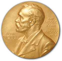
Esaki was born in Osaka, and studied physics at the University of Tokyo, where he received his B.Sc. in 1947 and his Ph.D. in 1959. He was awarded the Nobel Prize[2] for research conducted around 1958 regarding electron tunneling[3] in solids. He moved to the United States in 1960 and joined the IBM T. J. Watson Research Center, where he became an IBM Fellow in 1967. His first paper on the semiconductor superlattice[4] was published when he was with IBM. A 1987 comment by Esaki regarding the original paper on superlattices notes:
"The original version of the paper was rejected for publication by Physical Review on the referee's unimaginative assertion that it was 'too speculative' and involved 'no new physics.' However, this proposal was quickly accepted by the Army Research Office..."[5]
Subsequently, Esaki served as president of the University of Tsukuba[1] and Shibaura Institute of Technology. Since 2006 he is the President of the Yokohama College of Pharmacy. Esaki is also the recipient of The International Center in New York's Award of Excellence, the Order of Culture (1974) and the Grand Cordon of the Order of the Rising Sun (1998).
See also
References
- 1 2 3 4 Dr. Leo Esaki. japanprize.jp
- ↑ Esaki, Leo, "Long Journey into Tunneling," Nobel Lecture, December 12, 1973.
- ↑ Esaki, L. (1958). "New Phenomenon in Narrow Germanium p-n Junctions". Physical Review. 109 (2): 603. Bibcode:1958PhRv..109..603E. doi:10.1103/PhysRev.109.603.
- ↑ Esaki, L.; Tsu, R. (1970). "Superlattice and Negative Differential Conductivity in Semiconductors". IBM Journal of Research and Development. 14: 61. doi:10.1147/rd.141.0061.
- ↑ "This Weeks's Citation Classic", Current Contents No 28, July 13, 1987.
Further reading
- Large scale integrated circuits technology : state of the art and prospects : proceedings of the NATO Advanced Study Institute on "Large Scale Integrated Circuits Technology: State of the Art and Prospects," Erice, Italy, July 15–27, 1981 / edited by Leo Esaki and Giovanni Soncini (1982)
- Highlights in condensed matter physics and future prospects / edited by Leo Esaki (1991)
External links
| Wikimedia Commons has media related to Leo Esaki. |
- Leo Esaki – Biography. Retrieved August 5, 2003 from http://www.nobel.se/physics/laureates/1973/esaki-bio.html
- IBM record
- IEEE History Center – Leo Esaki. Retrieved July 19, 2011 from http://www.ieeeghn.org/wiki/index.php/Leo_Esaki
- Sony History – The Esaki Diode. Retrieved August 5, 2003 from http://www.sony.net/Fun/SH/1-7/h5.html
- Freeview video 'An Interview with Leo Esaki' by the Vega Science Trust
