Microstrip
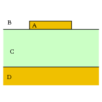
Microstrip is a type of electrical transmission line which can be fabricated using printed circuit board technology, and is used to convey microwave-frequency signals. It consists of a conducting strip separated from a ground plane by a dielectric layer known as the substrate. Microwave components such as antennas, couplers, filters, power dividers etc. can be formed from microstrip, with the entire device existing as the pattern of metallization on the substrate. Microstrip is thus much less expensive than traditional waveguide technology, as well as being far lighter and more compact. Microstrip was developed by ITT laboratories as a competitor to stripline (first published by Grieg and Engelmann in the December 1952 IRE proceedings[1]).
The disadvantages of microstrip compared with waveguide are the generally lower power handling capacity, and higher losses. Also, unlike waveguide, microstrip is not enclosed, and is therefore susceptible to cross-talk and unintentional radiation.
For lowest cost, microstrip devices may be built on an ordinary FR-4 (standard PCB) substrate. However it is often found that the dielectric losses in FR4 are too high at microwave frequencies, and that the dielectric constant is not sufficiently tightly controlled. For these reasons, an alumina substrate is commonly used.
On a smaller scale, microstrip transmission lines are also built into monolithic microwave integrated circuits.
Microstrip lines are also used in high-speed digital PCB designs, where signals need to be routed from one part of the assembly to another with minimal distortion, and avoiding high cross-talk and radiation.
Microstrip is very similar to stripline and coplanar waveguide, and it is possible to integrate all three on the same substrate.
A differential microstrip—a balanced signal pair of microstrip lines—is often used for high-speed signals such as DDR2 SDRAM clocks, USB Hi-Speed data lines, PCI Express data lines, LVDS data lines, etc., often all on the same PCB.[2][3][4] Most PCB design tools support such differential pairs.[5][6]
Inhomogeneity
The electromagnetic wave carried by a microstrip line exists partly in the dielectric substrate, and partly in the air above it. In general, the dielectric constant of the substrate will be different (and greater) than that of the air, so that the wave is travelling in an inhomogeneous medium. In consequence, the propagation velocity is somewhere between the speed of radio waves in the substrate, and the speed of radio waves in air. This behaviour is commonly described by stating the effective dielectric constant (or effective relative permittivity) of the microstrip; this being the dielectric constant of an equivalent homogeneous medium (i.e., one resulting in the same propagation velocity).
Further consequences of an inhomogeneous medium include:
- The line will not support a true TEM wave; at non-zero frequencies, both the E and H fields will have longitudinal components (a hybrid mode).[7] The longitudinal components are small however, and so the dominant mode is referred to as quasi-TEM.
- The line is dispersive. With increasing frequency, the effective dielectric constant gradually climbs towards that of the substrate, so that the phase velocity gradually decreases.[7][8] This is true even with a non-dispersive substrate material (the substrate dielectric constant will usually fall with increasing frequency).
- The characteristic impedance of the line changes slightly with frequency (again, even with a non-dispersive substrate material). The characteristic impedance of non-TEM modes is not uniquely defined, and depending on the precise definition used, the impedance of microstrip either rises, falls, or falls then rises with increasing frequency.[9] The low-frequency limit of the characteristic impedance is referred to as the quasi-static characteristic impedance, and is the same for all definitions of characteristic impedance.
- The wave impedance varies over the cross-section of the line.
Characteristic impedance
A closed-form approximate expression for the quasi-static characteristic impedance of a microstrip line was developed by Wheeler:[10][11][12]

where is the effective width, which is the actual width of the strip, plus a correction to account for the non-zero thickness of the metallization:


Here Z0 is the impedance of free space, εr is the relative permittivity of substrate, w is the width of the strip, h is the thickness ("height") of substrate, and t is the thickness of the strip metallization.
This formula is asymptotic to an exact solution in three different cases
- , any (parallel plate transmission line),
- , (wire above a ground-plane) and
- ,


It is claimed that for most other cases, the error in impedance is less than 1%, and is always less than 2%.[12] By covering all aspect-ratios in one formula, Wheeler 1977 improves on Wheeler 1965[11] which gives one formula for and another for (thus introducing a discontinuity in the result at ). Nevertheless, the 1965 paper is perhaps the more often cited. A number of other approximate formulae for the characteristic impedance have been advanced by other authors. However, most of these are applicable to only a limited range of aspect-ratios, or else cover the entire range piecewise.


Curiously, Harold Wheeler disliked both the terms 'microstrip' and 'characteristic impedance', and avoided using them in his papers.
Bends
In order to build a complete circuit in microstrip, it is often necessary for the path of a strip to turn through a large angle. An abrupt 90° bend in a microstrip will cause a significant portion of the signal on the strip to be reflected back towards its source, with only part of the signal transmitted on around the bend. One means of effecting a low-reflection bend, is to curve the path of the strip in an arc of radius at least 3 times the strip-width.[13] However, a far more common technique, and one which consumes a smaller area of substrate, is to use a mitred bend.
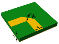
To a first approximation, an abrupt un-mitred bend behaves as a shunt capacitance placed between the ground plane and the bend in the strip. Mitring the bend reduces the area of metallization, and so removes the excess capacitance. The percentage mitre is the cut-away fraction of the diagonal between the inner and outer corners of the un-mitred bend.
The optimum mitre for a wide range of microstrip geometries has been determined experimentally by Douville and James.[14] They find that a good fit for the optimum percentage mitre is given by

subject to and with the substrate dielectric constant . This formula is entirely independent of . The actual range of parameters for which Douville and James present evidence is and . They report a VSWR of better than 1.1 (i.e., a return better than −26 dB) for any percentage mitre within 4% (of the original ) of that given by the formula. At the minimum of 0.25, the percentage mitre is 98.4%, so that the strip is very nearly cut through.


For both the curved and mitred bends, the electrical length is somewhat shorter than the physical path-length of the strip.
See also
- Distributed element filter
- Spurline, a microstrip notch-filter
References
- ↑ Grieg, D. D.; Engelmann, H. F. (Dec 1952). "Microstrip-A New Transmission Technique for the Klilomegacycle Range". Proceedings of the IRE. 40 (12): 1644–1650. doi:10.1109/JRPROC.1952.274144. ISSN 0096-8390.
- ↑ Olney, Barry. "Differential Pair Routing" (PDF). p. 51.
- ↑ Texas Instruments (2015). "High-Speed Interface Layout Guidelines" (PDF). p. 10. SPRAAR7E.
When possible, route high-speed differential pair signals on the top or bottom layer of the PCB with an adjacent GND layer. TI does not recommend stripline routing of the high-speed differential signals.
- ↑ Intel (2000). "High Speed USB Platform Design Guidelines" (PDF). p. 7.
- ↑ Silicon Labs. "USB Hardware Design Guide" (PDF). p. 9. AN0046.
- ↑ Kröger, Jens (2014). "Data Transmission at High Rates via Kapton Flexprints for the Mu3e Experiment" (PDF). pp. 19–21.
- 1 2 Denlinger, E. J. (January 1971). "A frequency dependent solution for microstrip transmission lines". IEEE Trans. Microwave Theory Tech. MTT-19: 30–39.
- ↑ Cory, H. (January 1981). "Dispersion characteristics of microstrip lines". IEEE Trans. Microwave Theory Tech. MTT-29: 59–61.
- ↑ Bianco, B.; Panini, L.; Parodi, M.; Ridetlaj, S. (March 1978). "Some considerations about the frequency dependence of the characteristic impedance of uniform microstrips". IEEE Trans. Microwave Theory Tech. MTT-26: 182–185.
- ↑ Wheeler, H. A. (May 1964). "Transmission-line properties of parallel wide strips by a conformal-mapping approximation". IEEE Trans. Microwave Theory Tech. MTT-12: 280–289.
- 1 2 Wheeler, H. A. (March 1965). "Transmission-line properties of parallel strips separated by a dielectric sheet". IEEE Tran. Microwave Theory Tech. MTT-13: 172–185.
- 1 2 Wheeler, H. A. (August 1977). "Transmission-line properties of a strip on a dielectric sheet on a plane". IEEE Tran. Microwave Theory Tech. MTT-25: 631–647.
- ↑ Lee, T. H. (2004). Planar Microwave Engineering. Cambridge University Press. pp. 173–174.
- ↑ Douville, R. J. P.; James, D. S. (March 1978). "Experimental study of symmetric microstrip bends and their compensation". IEEE Trans. Microwave Theory Tech. MTT-26: 175–182.