p–n junction

A p–n junction is a boundary or interface between two types of semiconductor material, p-type and n-type, inside a single crystal of semiconductor. The "p" (positive) side contains an excess of holes, while the "n" (negative) side contains an excess of electrons. The p-n junction is created by doping, for example by ion implantation, diffusion of dopants, or by epitaxy (growing a layer of crystal doped with one type of dopant on top of a layer of crystal doped with another type of dopant). If two separate pieces of material were used, this would introduce a grain boundary between the semiconductors that would severely inhibit its utility by scattering the electrons and holes.
p–n junctions are elementary "building blocks" of most semiconductor electronic devices such as diodes, transistors, solar cells, LEDs, and integrated circuits; they are the active sites where the electronic action of the device takes place. For example, a common type of transistor, the bipolar junction transistor, consists of two p–n junctions in series, in the form n–p–n or p–n–p.
The invention of the p–n junction is usually attributed to American physicist Russell Ohl of Bell Laboratories.[1] However, Vadim Lashkaryov reported discovery of p-n-junctions in CuO and silver sulphide photocells and selenium rectifiers in 1941.

A Schottky junction is a special case of a p–n junction, where metal serves the role of the p-type semiconductor.
Properties

The p–n junction possesses some interesting properties that have useful applications in modern electronics. A p-doped semiconductor is relatively conductive. The same is true of an n-doped semiconductor, but the junction between them can become depleted of charge carriers, and hence non-conductive, depending on the relative voltages of the two semiconductor regions. By manipulating this non-conductive layer, p–n junctions are commonly used as diodes: circuit elements that allow a flow of electricity in one direction but not in the other (opposite) direction. Bias is the application of a voltage across a p–n junction; forward bias is in the direction of easy current flow, and reverse bias is in the direction of little or no current flow.
Equilibrium (zero bias)
In a p–n junction, without an external applied voltage, an equilibrium condition is reached in which a potential difference is formed across the junction. This potential difference is called built-in potential .

After joining p-type and n-type semiconductors, electrons from the n region near the p–n interface tend to diffuse into the p region leaving behind positively charged ions in the n region and being recombined with holes, forming negatively charged ions in the p region. Likewise, holes from the p-type region near the p–n interface begin to diffuse into the n-type region, leaving behind negatively charged ions in the p region and recombining with electrons, forming positive ions in the n region. The regions near the p–n interface lose their neutrality and most of their mobile carriers, forming the space charge region or depletion layer (see figure A).
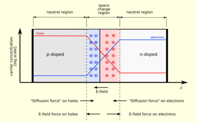
The electric field created by the space charge region opposes the diffusion process for both electrons and holes. There are two concurrent phenomena: the diffusion process that tends to generate more space charge, and the electric field generated by the space charge that tends to counteract the diffusion. The carrier concentration profile at equilibrium is shown in figure A with blue and red lines. Also shown are the two counterbalancing phenomena that establish equilibrium.

The space charge region is a zone with a net charge provided by the fixed ions (donors or acceptors) that have been left uncovered by majority carrier diffusion. When equilibrium is reached, the charge density is approximated by the displayed step function. In fact, since the y-axis of figure A is log-scale, the region is almost completely depleted of majority carriers (leaving a charge density equal to the net doping level), and the edge between the space charge region and the neutral region is quite sharp (see figure B, Q(x) graph). The space charge region has the same magnitude of charge on both sides of the p–n interfaces, thus it extends farther on the less doped side in this example (the n side in figures A and B).
Forward bias
In forward bias, the p-type is connected with the positive terminal and the n-type is connected with the negative terminal.

With a battery connected this way, the holes in the p-type region and the electrons in the n-type region are pushed toward the junction and start to neutralize the depletion zone, reducing its width. The positive potential applied to the p-type material repels the holes, while the negative potential applied to the n-type material repels the electrons. The change in potential between the p side and the n side decreases or switches sign. With increasing forward-bias voltage, the depletion zone eventually becomes thin enough that the zone's electric field cannot counteract charge carrier motion across the p–n junction, which as a consequence reduces electrical resistance. The electrons that cross the p–n junction into the p-type material (or holes that cross into the n-type material) will diffuse into the nearby neutral region. The amount of minority diffusion in the near-neutral zones determines the amount of current that may flow through the diode.
Only majority carriers (electrons in n-type material or holes in p-type) can flow through a semiconductor for a macroscopic length. With this in mind, consider the flow of electrons across the junction. The forward bias causes a force on the electrons pushing them from the N side toward the P side. With forward bias, the depletion region is narrow enough that electrons can cross the junction and inject into the p-type material. However, they do not continue to flow through the p-type material indefinitely, because it is energetically favorable for them to recombine with holes. The average length an electron travels through the p-type material before recombining is called the diffusion length, and it is typically on the order of micrometers.[2]
Although the electrons penetrate only a short distance into the p-type material, the electric current continues uninterrupted, because holes (the majority carriers) begin to flow in the opposite direction. The total current (the sum of the electron and hole currents) is constant in space, because any variation would cause charge buildup over time (this is Kirchhoff's current law). The flow of holes from the p-type region into the n-type region is exactly analogous to the flow of electrons from N to P (electrons and holes swap roles and the signs of all currents and voltages are reversed).
Therefore, the macroscopic picture of the current flow through the diode involves electrons flowing through the n-type region toward the junction, holes flowing through the p-type region in the opposite direction toward the junction, and the two species of carriers constantly recombining in the vicinity of the junction. The electrons and holes travel in opposite directions, but they also have opposite charges, so the overall current is in the same direction on both sides of the diode, as required.
The Shockley diode equation models the forward-bias operational characteristics of a p–n junction outside the avalanche (reverse-biased conducting) region.
Reverse bias

Connecting the p-type region to the negative terminal of the battery and the n-type region to the positive terminal corresponds to reverse bias. If a diode is reverse-biased, the voltage at the cathode is comparatively higher than at the anode. Therefore, very little current will flow until the diode breaks down. The connections are illustrated in the adjacent diagram.
Because the p-type material is now connected to the negative terminal of the power supply, the 'holes' in the p-type material are pulled away from the junction, leaving behind charged ions and causing the width of the depletion region to increase. Likewise, because the n-type region is connected to the positive terminal, the electrons will also be pulled away from the junction, with similar effect. This increases the voltage barrier causing a high resistance to the flow of charge carriers, thus allowing minimal electric current to cross the p–n junction. The increase in resistance of the p–n junction results in the junction behaving as an insulator.
The strength of the depletion zone electric field increases as the reverse-bias voltage increases. Once the electric field intensity increases beyond a critical level, the p–n junction depletion zone breaks down and current begins to flow, usually by either the Zener or the avalanche breakdown processes. Both of these breakdown processes are non-destructive and are reversible, as long as the amount of current flowing does not reach levels that cause the semiconductor material to overheat and cause thermal damage.
This effect is used to advantage in Zener diode regulator circuits. Zener diodes have a low breakdown voltage. A standard value for breakdown voltage is for instance 5.6 V. This means that the voltage at the cathode cannot be more than about 5.6 V higher than the voltage at the anode (although there is a slight rise with current), because the diode will break down – and therefore conduct – if the voltage gets any higher. This in effect limits the voltage over the diode.
Another application of reverse biasing is Varicap diodes, where the width of the depletion zone (controlled with the reverse bias voltage) changes the capacitance of the diode.
Governing equations
Size of depletion region
For a p–n junction, letting and be the concentrations of acceptor and donor atoms respectively, and letting and be the equilibrium concentrations of electrons and holes respectively, yields, by Poisson's equation:


![-\frac{\mathrm{d}^2 V}{\mathrm{d}x^2}=\frac{\rho }{\varepsilon }=\frac{q}{\varepsilon }\left[ (N_0-P_0)+(C_D-C_A)\right]](../I/m/8d2e818fcbd8e62ae5ea74b96ad410f253f2bf7d.svg)
where is the electric potential, is the charge density, is permittivity and is the magnitude of the electron charge. Letting be the width of the depletion region within the p-side, and letting be the width of the depletion region within the n-side, it must be that


because the total charge on either side of the depletion region must cancel out. Therefore, letting and represent the entire depletion region and the potential difference across it,


![\Delta V=\int_D \int\frac{q}{\varepsilon }\left[ (N_0-P_0)+(C_D-C_A)\right]\,\mathrm{d} x\,\mathrm{d}x](../I/m/f19567fd064eabeaf83e8ee5cff08a6f449ca8e4.svg)

where , because we are in the depletion region. And thus, letting be the total width of the depletion region, we get


can be written as , where we have broken up the voltage difference into the equilibrium plus external components. The equilibrium potential results from diffusion forces, and thus we can calculate by implementing the Einstein relation and assuming the semiconductor is nondegenerate (i.e. the product is independent of the Fermi energy):


where T is the temperature of the semiconductor and k is Boltzmann constant.[3]
Current across depletion region
The Shockley ideal diode equation characterizes the current across a p–n junction as a function of external voltage and ambient conditions (temperature, choice of semiconductor, etc.). To see how it can be derived, we must examine the various reasons for current. The convention is that the forward (+) direction be pointed against the diode's built-in potential gradient at equilibrium.
- Forward Current ()
- Diffusion Current: current due to local imbalances in carrier concentration , via the equation
- Reverse Current ()
- Field Current
- Generation Current


Summary
The forward-bias and the reverse-bias properties of the p–n junction imply that it can be used as a diode. A p–n junction diode allows electric charges to flow in one direction, but not in the opposite direction; negative charges (electrons) can easily flow through the junction from n to p but not from p to n, and the reverse is true for holes. When the p–n junction is forward-biased, electric charge flows freely due to reduced resistance of the p–n junction. When the p–n junction is reverse-biased, however, the junction barrier (and therefore resistance) becomes greater and charge flow is minimal.
Non-rectifying junctions
In the above diagrams, contact between the metal wires and the semiconductor material also creates metal–semiconductor junctions called Schottky diodes. In a simplified ideal situation a semiconductor diode would never function, since it would be composed of several diodes connected back-to-front in series. But, in practice, surface impurities within the part of the semiconductor that touches the metal terminals will greatly reduce the width of those depletion layers to such an extent that the metal-semiconductor junctions do not act as diodes. These non-rectifying junctions behave as ohmic contacts regardless of applied voltage polarity.
See also
| Wikimedia Commons has media related to PN-junction diagrams. |
References
- ↑ Riordan, Michael; Lillian Hoddeson (1988). Crystal fire: the invention of the transistor and the birth of the information age. USA: W. W. Norton & Company. pp. 88–97. ISBN 0-393-31851-6.
- ↑ Hook, J. R.; H. E. Hall (2001). Solid State Physics. John Wiley & Sons. ISBN 0-471-92805-4.
- ↑ Luque, Antonio; Steven Hegedus (29 March 2011). Handbook of Photovoltaic Science and Engineering. John Wiley & Sons. ISBN 978-0-470-97612-8.
Further reading
- Shockley, William (1949). "The Theory of p-n Junctions in Semiconductors and p-n Junction Transistors". Bell System Technical Journal. 28 (3): 435–489. doi:10.1002/j.1538-7305.1949.tb03645.x.
External links
- V. E. Lashkaryov, Investigation of a barrier layer by the thermoprobe method, Izv. Akad. Nauk SSSR, Ser. Fiz. 5, 442-446 (1941), English translation: Ukr. J. Phys. 53, 53-56 (2008),http://ujp.bitp.kiev.ua/files/journals/53/si/53SI11p.pdf. Report on discovery of p-n-junctions.
- https://www.youtube.com/watch?v=JBtEckh3L9Q Educational video on the P-N junction.
- "P-N Junction" – PowerGuru, August, 2012.
- Olav Torheim, Elementary Physics of P-N Junctions, 2007.
- PN Junction Properties Calculator
- PN Junction Lab free to use on nanoHUB.org allows simulation and study of a p–n junction diode with different doping and materials. Users can calculate current-voltage (I-V) & capacitance-voltage (C-V) outputs, as well.
- Understanding the PN Junction – Explains PN junction in a very easy to understand language.