Pascal (microarchitecture)
|
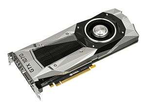
The GTX 1070, the second commercial card to use the Pascal architecture | |
| Fabrication process | 16 nm |
|---|---|
| History | |
| Predecessor | Maxwell |
| Successor | Volta |
Pascal is the codename for a GPU microarchitecture developed by Nvidia as the successor to the Maxwell microarchitecture. The Pascal microarchitecture was introduced April 2016 with the GP100 chip. The architecture is named after Blaise Pascal, the 17th century mathematician.
Details
On May 27, 2016 the GP104 chip to be found on the GeForce GTX 10XX branded graphics cards. Graphics cards are part of the GeForce 10 series.
In March 2014, Nvidia announced that the successor to Maxwell would be the Pascal microarchitecture; announced on the 6th May 2016 and released on the 27th May 2016. The Tesla P100 (GP100 chip) has a different version of the Pascal architecture compared to the GTX GPUs (GP104 chip). The shader units in GP104 have a rather Maxwell-like design.[1]
Architectural improvements of the GP100 architecture include the following:[2][3][4]
- In Pascal, an SM (streaming multiprocessor) consists of 64 CUDA cores. Maxwell packed 128, Kepler 192, Fermi 32 and Tesla only 8 CUDA cores into an SM; the GP100 SM is partitioned into two processing blocks, each having 32 single-precision CUDA Cores, an instruction buffer, a warp scheduler, 2 texture mapping units and 2 dispatch units.
- CUDA Compute Capability 6.0.
- High Bandwidth Memory 2 — some cards feature 16 GiB HBM2 in four stacks with a total of 4096bit bus with a memory bandwidth of 720 GB/s.
- Unified memory — a memory architecture, where the CPU and GPU can access both main system memory and memory on the graphics card with the help of a technology called "Page Migration Engine".
- NVLink — a high-bandwidth bus between the CPU and GPU, and between multiple GPUs. Allows much higher transfer speeds than those achievable by using PCI Express; estimated to provide between 80 and 200 GB/s.[5][6]
- 16-bit (FP16) floating-point operations (colloquially "half precision") can be executed at twice the rate of 32-bit floating-point operations ("single precision")[7] and 64-bit floating-point operations (colloquially "double precision") executed at half the rate of 32-bit floating point operations.[8]
- More registers — twice the amount of registers per CUDA core compared to Maxwell.
- More shared memory.
- Dynamic load balancing scheduling system.[9] This allows the scheduler to dynamically adjust the amount of the GPU assigned to multiple tasks, ensuring that the GPU remains saturated with work except when there is no more work that can safely be distributed to distribute.[9] Nvidia therefore has safely enabled asynchronous compute in Pascal's driver.[9]
- Instruction-level and thread-level preemption.[10]
Architectural improvements of the GP104 architecture include the following:[1]
- CUDA Compute Capability 6.1.
- GDDR5X — new memory standard supporting 10Gbit/s data rates, updated memory controller.[11]
- Simultaneous Multi-Projection - generating multiple projections of a single geometry stream, as it enters the SMP engine from upstream shader stages.[12]
- DisplayPort 1.4, HDMI 2.0b.
- Fourth generation Delta Color Compression.
- Enhanced SLI Interface — SLI interface with higher bandwidth compared to the previous versions.
- PureVideo Feature Set H hardware video decoding HEVC Main10(10bit), Main12(12bit) and VP9 hardware decoding.
- HDCP 2.2 support for 4K DRM protected content playback and streaming (Maxwell GM200 and GM204 lack HDCP 2.2 support, GM206 supports HDCP 2.2).[13]
- NVENC HEVC Main10 10bit hardware encoding.
- GPU Boost 3.0.
- Asynchronous compute.[14]
- Instruction-level preemption.[10] In graphics tasks, the driver restricts this to pixel-level preemption because pixel tasks typically finish quickly and the overhead costs of doing pixel-level preemption are much lower than performing instruction-level preemption.[10] Compute tasks get thread-level or instruction-level preemption.[10] Instruction-level preemption is useful because compute tasks can take long times to finish and there are no guarantees on when a compute task finishes, so the driver enables the very expensive instruction-level preemption for these tasks.[10]
Overview
Graphics Processor Cluster
A chip is partitioned into Graphics Processor Clusters (GPCs). For the GP104 chips, a GPC engulfs 5 SMs.
Streaming Multiprocessor "Pascal"
A "Streaming Multiprocessor" corresponds to AMD's Compute Unit. An SMP encompasses 128 single-precision ALUs ("CUDA cores") on GP104 chips and 64 single-precision ALUs on GP100 chips.
What AMD calls a CU (compute unit) can be compared to what Nvidia calls an SM (streaming multiprocessor). While all CU versions consist of 64 shader processors (i.e. 4 SIMD Vector Units (each 16-lane wide)= 64), Nvidia (regularly calling shader processors "CUDA cores") experimented with very different numbers:
- One Tesla SM combines 8 single-precision (FP32) shader processors
- One Fermi SM combines 32 single-precision (FP32) shader processors
- One Kepler SM combines 192 single-precision (FP32) shader processors and also 64 double-precision units (at least the GK110 GPUs)
- One Maxwell SM combines 128 single-precision (FP32) shader processors
- One Pascal SM on the GP100 combines 64 single-precision (FP32) shader processors and also 32 double-precision (FP64) (at least the GP100 GPUs) providing a 2:1 ratio of single- to double-precision throughput. On the GP104 an SM combines 128 single-precision ALUs, 4 double-precision ALUs providing a 32:1 ratio, and one half-precision ALU that contains a vector of two half-precision floats which can execute the same instruction on both floats providing a 64:1 ratio if the same instruction is used on both elements. GP100 however uses more flexible FP32 cores that are able to process one single-precision or two half-precision numbers in a two-element vector.[15] Nvidia intends to address the calculation of algorithms related to deep learning with those.
Polymorph-Engine 4.0
The Polymorph Engine version 4.0 is the unit responsible for Tessellation. It corresponds functionally with AMD's Geometric Processor. It has been moved from the shader module to the TPC to allow one Polymorph engine to feed multiple SMs within the TPC.[16]
Chips
- GP100: Nvidia Tesla P100 GPU accelerator is targeted at GPGPU applications such as FP64 double precision compute and deep learning training that uses FP16. It uses HBM2 memory.[17]
- GP102: This GPU is used in the Titan X[18] and has 12GB of GDDR5X memory, 384bit memory bus and 480GB/s of memory bandwidth. It is also used in the Quadro P6000[19] and Tesla P40.[20]
- GP104: This GPU is used in the GeForce GTX 1070 and the GTX 1080. The GTX 1070 has 1/4 of its shaders disabled and is connected to GDDR5 memory, while the GTX 1080 is a full chip and is connected to GDDR5X memory. It is also used in the Quadro P5000 and Tesla P4.
- GP106: This GPU is used in the GeForce GTX 1060 with GDDR5 memory.[21][22]
- GP107: This GPU is used in the GeForce GTX 1050 Ti and GeForce GTX 1050.
- GP108 (rumored).[23]
On the GP104 chip an SM consists of 128 single-precision ALUs ("CUDA cores"), on the GP100 of 64 single-precision ALUs. Due to different organization of the chips, like number of double precision ALUs, the theoretical double precision performance of the GP100 is half of the theoretical one for single precision; the ratio is 1/32 for the GP104 chip.
| GK104 | GK110 | GM204 (GTX 970) | GM204 (GTX 980) | GM200 | GP104 | GP100 | |
|---|---|---|---|---|---|---|---|
| Dedicated texture cache per SM | 48 KiB | N/A | N/A | N/A | N/A | N/A | N/A |
| Texture (graphics or compute) or read-only data (compute only) cache per SM | N/A | 48 KiB[24] | N/A | N/A | N/A | N/A | N/A |
| Programmer-selectable shared memory/L1 partitions per SM | 48 KiB shared memory + 16 KiB L1 cache (default)[25] | 48 KiB shared memory + 16 KiB L1 cache (default)[25] | N/A | N/A | N/A | N/A | N/A |
| 32 KiB shared memory + 32 KiB L1 cache[25] | 32 KiB shared memory + 32 KiB L1 cache[25] | ||||||
| 16 KiB shared memory + 48 KiB L1 cache[25] | 16 KiB shared memory + 48 KiB L1 cache[25] | ||||||
| Unified L1 cache/texture cache per SM | N/A | N/A | 48 KiB[26] | 48 KiB[26] | 48 KiB[26] | 48 KiB[26] | 24 KiB[26] |
| Dedicated shared memory per SM | N/A | N/A | 96 KiB[26] | 96 KiB[26] | 96 KiB[26] | 96 KiB[26] | 64 KiB[26] |
| L2 cache per chip | 512 KiB[26] | 1536 KiB[26] | 1792 KiB[27] | 2048 KiB[27] | 2048 KiB[26] | 2048 KiB[26] | 4096 KiB[26] |
Performance
The theoretical single-precision processing power of a Pascal GPU in GFLOPS is computed as 2 (operations per FMA instruction per CUDA core per cycle) × number of CUDA cores × core clock speed (in GHz).
The theoretical double-precision processing power of a Pascal GPU is 1/2 of the single precision performance on GP100, and 1/32 on GP102 and GP104.
The theoretical half-precision processing power of a Pascal GPU is 2× of the single precision performance on GP100[8] and 1/64 on GP104.[15]
Successor
After Pascal, the next architecture will be preliminary codenamed Volta.[28] Nvidia announced that the Volta GPU would feature High Bandwidth Memory, Unified Memory, and NVLink.[28]
See also
References
- 1 2 "NVIDIA GeForce GTX 1080" (PDF). International.download.nvidia.com. Retrieved 2016-09-15.
- ↑ Gupta, Sumit (2014-03-21). "NVIDIA Updates GPU Roadmap; Announces Pascal". Blogs.nvidia.com. Retrieved 2014-03-25.
- ↑ "Parallel Forall". NVIDIA Developer Zone. Devblogs.nvidia.com. Retrieved 2014-03-25.
- ↑ "NVIDIA Tesla P100" (PDF). International.download.nvidia.com. Retrieved 2016-09-15.
- ↑ "nside Pascal: NVIDIA's Newest Computing Platform". 2016-04-05.
- ↑ Denis Foley (2014-03-25). "NVLink, Pascal and Stacked Memory: Feeding the Appetite for Big Data". nvidia.com. Retrieved 2014-07-07.
- ↑ "NVIDIA's Next-Gen Pascal GPU Architecture to Provide upto 10X Speedup for Deep Learning Apps". The Official NVIDIA Blog. Retrieved 23 March 2015.
- 1 2 Smith, Ryan (2015-04-05). "NVIDIA Announces Tesla P100 Accelerator - Pascal GP100 Power for HPC". AnandTech. Retrieved 2016-05-27.
Each of those SMs also contains 32 FP64 CUDA cores - giving us the 1/2 rate for FP64 - and new to the Pascal architecture is the ability to pack 2 FP16 operations inside a single FP32 CUDA core under the right circumstances
- 1 2 3 Smith, Ryan (July 20, 2016). "The NVIDIA GeForce GTX 1080 & GTX 1070 Founders Editions Review: Kicking Off the FinFET Generation". AnandTech. p. 9. Retrieved July 21, 2016.
- 1 2 3 4 5 Smith, Ryan (July 20, 2016). "The NVIDIA GeForce GTX 1080 & GTX 1070 Founders Editions Review: Kicking Off the FinFET Generation". AnandTech. p. 10. Retrieved July 21, 2016.
- ↑ "GTX 1080 Graphics Card". GeForce. Retrieved 2016-09-15.
- ↑ Carbotte, Kevin (2016-05-17). "Nvidia GeForce GTX 1080 Simultaneous Multi-Projection & Async Compute". Tomshardware.com. Retrieved 2016-09-15.
- ↑ "Nvidia Pascal HDCP 2.2". Nvidia Hardware Page. Retrieved 2016-05-08.
- ↑ Shrout, Ryan (July 14, 2016). "3DMark Time Spy: Looking at DX12 Asynchronous Compute Performance". PC Perspective. Retrieved July 14, 2016.
- 1 2 Smith, Ryan (July 20, 2016). "The NVIDIA GeForce GTX 1080 & GTX 1070 Founders Editions Review: Kicking Off the FinFET Generation". AnandTech. p. 5. Retrieved July 21, 2016.
- ↑ Smith, Ryan (July 20, 2016). "The NVIDIA GeForce GTX 1080 & GTX 1070 Founders Editions Review: Kicking Off the FinFET Generation". AnandTech. p. 4. Retrieved July 21, 2016.
- ↑ Harris, Mark (April 5, 2016). "Inside Pascal: NVIDIA's Newest Computing Platform". Parallel Forall. Nvidia. Retrieved June 3, 2016.
- ↑ "NVIDIA TITAN X Graphics Card with Pascal". GeForce. Retrieved 2016-09-15.
- ↑ "New Quadro Graphics Built on Pascal Architecture". NVIDIA. Retrieved 2016-09-15.
- ↑ "Accelerating Data Center Workloads with GPUs". NVIDIA. Retrieved 2016-09-15.
- ↑ "NVIDIA GeForce GTX 1060 to be released on July 7th". VideoCardz.com. Retrieved 2016-09-15.
- ↑ "GTX 1060 Graphics Cards". GeForce. Retrieved 2016-09-15.
- ↑ "AIDA64 - Ever wondered how big the new #nVIDIA #Pascal GPU...". May 25, 2016. Retrieved June 5, 2016.
- ↑ Smith, Ryan (November 12, 2012). "NVIDIA Launches Tesla K20 & K20X: GK110 Arrives At Last". AnandTech. p. 3. Retrieved July 24, 2016.
- 1 2 3 4 5 6 Nvidia (September 1, 2015). "CUDA C Programming Guide". Retrieved July 24, 2016.
- 1 2 3 4 5 6 7 8 9 10 11 12 13 14 15 Triolet, Damien (May 24, 2016). "Nvidia GeForce GTX 1080, le premier GPU 16nm en test !". Hardware.fr (in French). p. 2. Retrieved July 24, 2016.
- 1 2 Smith, Ryan (January 26, 2015). "GeForce GTX 970: Correcting The Specs & Exploring Memory Allocation". AnandTech. p. 1. Retrieved July 24, 2016.
- 1 2 "NVIDIA Updates GPU Roadmap; Announces Pascal". The Official NVIDIA Blog.