Signetics 8X300

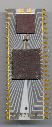
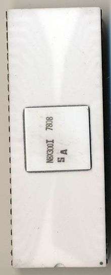
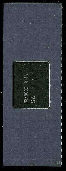

The 8X300 is a microprocessor produced and marketed by Signetics starting 1976 as a second source for the SMS 300 by Scientific Micro Systems, Inc.[1][2][3]
Although SMS developed the SMS 300 / 8X300 products, Signetics was the sole manufacturer of this product line. In 1978 Signetics purchased the rights to the SMS300 series and renamed the SMS300 to 8X300
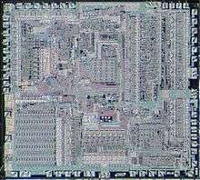
It was designed to be a fast microcontroller and signal processor, and because of this differs considerably from conventional NMOS logic microprocessors of the time. Perhaps the major difference was that it was implemented with bipolar Schottky transistor technology, and could fetch, decode and execute an instruction in only 250 ns. Data could be input from one device, modified, and output to another device during one instruction cycle.
In 1982, Signetics released an improved and faster version, the 8X305. This processor went on to become very popular in military applications and was second-sourced by Advanced Micro Devices as the AM29X305. Eventually, production rights were sold to Lansdale Semiconductor Inc., who was still offering the 8X305 as of 2016.
Architecture
The device was supplied in a 50-pin DIL ceramic package, and ran from a single 5V supply rail. An external pass transistor was required to complete an on-chip voltage regulator, which supplied 3V to selected areas of the chip. This helped to maintain the total current drain of the chip to less than 450mA.
Clock requirements were met by connecting an 8 MHz crystal directly to two pins. Alternatively, out of phase signals from an external clock generator could be used.
A second unique feature is a dedicated 13 bit address and 16 bit databus to access program memory, allowing 8192 16-bit program words to be directly addressed. This allowed ROM / PROM program memories to be directly connected without further hardware. A second combined 8-bit address/data bus- the interface vector (IV) bus, was used for data and I/O. Two control signals - WC (write command) and SC (select command) determined the state of the IV bus as follows:
- SC=1, WC=0 I/O address is being output on the IV bus
- SC=0, WC=1 I/O data is being output on the IV bus
- SC=0, WC=0 I/O input data is being expected on the IV bus
A further two signals; LB (left bank select) and RB (right bank select) effectively doubled the IV bus address space, and were most often used to switch between RAM memory in one bank and I/O ports in the other.
Another unusual feature was that rather than execute mask, rotate, shift and merge instructions in the arithmetic logic unit (ALU), as is the case with most microprocessors, the 8X300 had separate mask, rotate, shift and merge units. Data could therefore be rotated, masked, modified, shifted and merged (in that order), all in one instruction cycle.
Instruction set
The processor normally manipulates 8-bit data bytes, but the mask unit makes it possible to manipulate single or multiple bits, making this a variable data-length processor. Internal data is stored in 8-bit read/write registers—R1 through R6,R9, and an auxiliary register (R0). The auxiliary register holds one of the operands used in two-operand instructions, such as ADD or AND, and a single-bit (read only) overflow register (R8) stores the carry-over bit from add operations. Two virtual write only registers IVL (R7) and IVR (R15) are used to put an address on the IV bus, and two sets of eight virtual registers (R16-R23 and R24-R31) are used to transfer data to or from the IV bus. In the latter case, the upper two bits of the register number select the left or right bank, and the lower three bits define the number of places the data is to be rotated. An 8-bit IV-bus buffer retains a copy of the last data to be transferred to or from the IV-bus. This data is used in Merge operations.
The three most significant bits of the instruction define the opcode, and divide the instructions into 8 classes:
- The MOVE instruction allows the contents of selected registers to be copied, placed on the IV bus, or vice versa.
- The ADD, AND and XOR classes are similar, except that with these instructions the contents of the auxiliary register are combined with the source register before the MOVE part of the instruction is executed.
- The XEC instruction allows a selected instruction at a different address to be executed without incrementing the program counter.
- The NZT instruction allows a conditional branch to be implemented.
- The XMIT instruction allows an 8-bit binary pattern specified in the instruction to be placed in a specified register or on the IV bus. It is similar to a load-immediate instruction.
- The JMP instruction performs an unconditional branch to anywhere within the 8192 word program memory
The use of the remaining 13 bits of the instruction depends on the opcode:
- MOVE, AND, ADD and XOR instructions: 5 bits are used to define the source register, 3 bits are used to define any rotate or mask operation (the R/L field), and the remaining 5 bits define the destination register.
- XEC and NZT: 5 bits are used to define the source register, the remaining 8 bits define the address field.
- XEC: the contents of the source register are first added to the address field, which is then used as the lower 8 bits of the program address.
- NZT: the jump is taken if the source register is non-zero. If the jump is taken, the address field is used as the lower 8 bits of the program address.
- XMIT: 5 bits are used to define the destination register, the remaining 8 bits define the data.
- JMP: all 13 bits are used as an absolute address in program memory.
Shift, rotate, mask and merge
The rotate and mask units are located between the register bank and the ALU. Therefore, all data can, in principle, be rotated and masked before it enters the ALU.
- Rotate Unit: This unit will Rotate the data to the RIGHT by the number of places specified in the opcode.
- Mask Unit: This unit will mask off (set to zero) the upper bits of the data so as to retain the number of lower bits specified in the opcode.
The Shift and Merge units are located between the ALU and the IV-bus, and any data sent to IV-bus can therefore be shifted and merged before being output.
- Shift Unit: This unit will shift the data to the LEFT the number of places specified in the opcode.
- Merge Unit: This unit will Merge (replace) the number of bits specified by the opcode in the IV-bus buffer with the data with before placing the contents of the buffer on the IV-bus.
Note: a count of zero for the number of bits to merge will result in all 8 bits being replaced.
The following combinations are possible, depending on the source and destination:
- MOVE, ADD, AND and XOR instructions:
- register to register (including IVL and IVR registers): Rotate
- register to IV-bus (data output): shift and merge
- IV-bus input to register: rotate and mask
- IV-bus input to IV-bus output: rotate, mask, shift and merge
- IV-bus input to IVL or IVR register (IV-bus address output): rotate and mask
- XEC and NZT:
- IV-bus input: rotate and mask
- XMIT
- IV-bus (data output): shift and merge
I/O
Transferring data to and from the 8X300 is a two-step process:
- 1 Using one of the MOVE, ADD, AND, XOR or XMT instructions and specifying one of the virtual registers IVL (left bank) or IVR (right bank) as the destination, an address is output on the IV bus, along with Select Command and Bank Select signals.
Because the I/O address is output separately, the I/O ports must hold (latch) the selection. This can be done with separate address decoders and latches, or with an I/O port with integrated address decoding and latching, such as the 8X32. Because of the latching, I/O ports, once addressed, remain active until a different address is output, and can be accessed multiple times without the need to address them again. Two I/O ports (or RAM addresses) can be active at the same time, using the bank select signals to rapidly switch between them without further addressing.
- 2 Data is transferred to or from the 8X300 using one of the MOVE, ADD, AND or XOR instructions and specifying one of the registers R16-R31 as the source and/or destination. The register chosen defines which bank select signal accompanies the transfer.
Applications
In an extensive application note Signetics showed how to use the 8X300 as a floppy disk controller. A revised application note showed the use of the 8X300 together with the 8X330. Other application notes described:
- A teletype multiplexor
- A data concentrator
- A remote terminal controller
- A computer I/O bus emulator
- Interfacing RAM memory
A demonstration system (contained in a briefcase) and application note showed the 8X300 being used in a traffic-light controller
Support devices
- 8X01 Cyclic redundancy checker
- 8X31 / 8T31 8-bit latched bidirectional I/O port
- 8X32/8X36/8X42 8-bit latched addressable bidirectional I/O port
- 8T39 Addressable bus expander
- 8X41 Asynchronous bidirectional bus extender and repeater (SABER)
- 8T58 Transparent bus expander
- 8X320 Bus interface register array
- 8X330 floppy disk formatter/controller
- 8X350 2048-bit bipolar RAM (256*8) 35nS access time
- SMS360/8X360 Interface vector byte