TRIAC

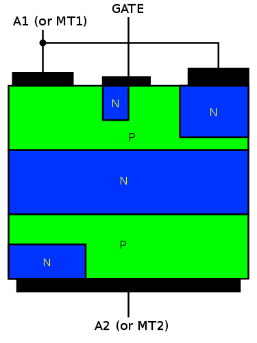
TRIAC, from triode for alternating current, is a generic trademark for a three terminal electronic component that conducts current in either direction when triggered. Its formal name is bidirectional triode thyristor or bilateral triode thyristor. A thyristor is analogous to a relay in that a small voltage and current can control a much larger voltage and current. The illustration on the right shows the circuit symbol for a TRIAC where A1 is Anode 1, A2 is Anode 2, and G is Gate. Anode 1 and Anode 2 are normally termed Main Terminal 1 (MT1) and Main Terminal 2 (MT2) respectively.
TRIACs are a subset of thyristors and are related to silicon controlled rectifiers (SCRs). TRIACs differ from SCRs in that they allow current flow in both directions, whereas an SCR can only conduct current in a single direction. Most TRIACs can be triggered by applying either a positive or negative voltage to the gate (an SCR requires a positive voltage). Once triggered, SCRs and TRIACs continue to conduct, even if the gate current ceases, until the main current drops below a certain level called the holding current.
Gate turn-off thyristors (GTOs) are similar to TRIACs but provide more control by turning off when the gate signal ceases.
TRIACs bidirectionality makes them convenient switches for alternating-current (AC). In addition, applying a trigger at a controlled phase angle of the AC in the main circuit allows control of the average current flowing into a load (phase control). This is commonly used for controlling the speed of induction motors, dimming lamps, and controlling electric heaters.
Operation
|
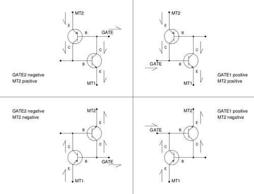
To understand how TRIACs work, consider the triggering in each of the four quadrants. The four quadrants are illustrated in Figure 1, and depend on the gate and MT2 voltages with respect to MT1. Main Terminal 1 (MT1) and Main Terminal (MT2) are also referred to as Anode 1 (A1) and Anode 2 (A2) respectively.[1]
The relative sensitivity depends on the physical structure of a particular triac, but as a rule, quadrant I is the most sensitive (least gate current required), and quadrant 4 is the least sensitive (most gate current required).
In quadrants 1 and 2, MT2 is positive, and current flows from MT2 to MT1 through P, N, P and N layers. The N region attached to MT2 does not participate significantly. In quadrants 3 and 4, MT2 is negative, and current flows from MT1 to MT2, also through P, N, P and N layers. The N region attached to MT2 is active, but the N region attached to MT1 only participates in the initial triggering, not the bulk current flow.
In most applications, the gate current comes from MT2, so quadrants 1 and 3 are the only operating modes (both gate and MT2 positive or negative against MT1). Other applications with single polarity triggering from an IC or digital drive circuit operate in quadrants 2 and 3, than MT1 is usually connected to positive voltage (e.g. +5V) and gate is pulled down to 0V (ground).
Quadrant 1
|
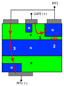
Quadrant 1 operation occurs when the gate and MT2 are positive with respect to MT1.Figure 1
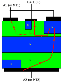
The mechanism is illustrated in Figure 3. The gate current makes an equivalent NPN transistor switch on, which in turn draws current from the base of an equivalent PNP transistor, turning it on also. Part of the gate current (dotted line) is lost through the ohmic path across the p-silicon, flowing directly into MT1 without passing through the NPN transistor base. In this case, the injection of holes in the p-silicon makes the stacked n, p and n layers beneath MT1 behave like a NPN transistor, which turns on due to the presence of a current in its base. This, in turn, causes the p, n and p layers over MT2 to behave like a PNP transistor, which turns on because its n-type base becomes forward-biased with respect to its emitter (MT2). Thus, the triggering scheme is the same as an SCR. The equivalent circuit is depicted in Figure 4.
However, the structure is different from SCRs. In particular, TRIAC always has a small current flowing directly from the gate to MT1 through the p-silicon without passing through the p-n junction between the base and the emitter of the equivalent NPN transistor. This current is indicated in Figure 3 by a dotted red line and is the reason why a TRIAC needs more gate current to turn on than a comparably rated SCR.[2]
Generally, this quadrant is the most sensitive of the four. This is because it is the only quadrant where gate current is injected directly into the base of one of the main device transistors.
Quadrant 2
|
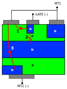
Quadrant 2 operation occurs when the gate is negative and MT2 is positive with respect to MT1.Figure 1
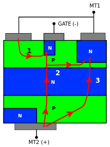
Figure 5 shows the triggering process. The turn-on of the device is three-fold and starts when the current from MT1 flows into the gate through the p-n junction under the gate. This switches on a structure composed by an NPN transistor and a PNP transistor, which has the gate as cathode (the turn-on of this structure is indicated by "1" in the figure). As current into the gate increases, the potential of the left side of the p-silicon under the gate rises towards MT1, since the difference in potential between the gate and MT2 tends to lower: this establishes a current between the left side and the right side of the p-silicon (indicated by "2" in the figure), which in turn switches on the NPN transistor under the MT1 terminal and as a consequence also the pnp transistor between MT2 and the right side of the upper p-silicon. So, in the end, the structure which is crossed by the major portion of the current is the same as quadrant-I operation ("3" in Figure 5).[2]
Quadrant 3
|
Quadrant 3 operation occurs when the gate and MT2 are negative with respect to MT1.Figure 1
The whole process is outlined in Figure 6. The process happens in different steps here too. In the first phase, the pn junction between the MT1 terminal and the gate becomes forward-biased (step 1). As forward-biasing implies the injection of minority carriers in the two layers joining the junction, electrons are injected in the p-layer under the gate. Some of these electrons do not recombine and escape to the underlying n-region (step 2). This in turn lowers the potential of the n-region, acting as the base of a pnp transistor which switches on (turning the transistor on without directly lowering the base potential is called remote gate control). The lower p-layer works as the collector of this PNP transistor and has its voltage heightened: actually, this p-layer also acts as the base of an NPN transistor made up by the last three layers just over the MT2 terminal, which, in turn, gets activated. Therefore, the red arrow labeled with a "3" in Figure 6 shows the final conduction path of the current.[2]
Quadrant 4
|
Quadrant 4 operation occurs when the gate is positive and MT2 is negative with respect to MT1. Figure 1
Triggering in this quadrant is similar to triggering in quadrant III. The process uses a remote gate control and is illustrated in Figure 7. As current flows from the p-layer under the gate into the n-layer under MT1, minority carriers in the form of free electrons are injected into the p-region and some of them are collected by the underlying n-p junction and pass into the adjoining n-region without recombining. As in the case of a triggering in quadrant III, this lowers the potential of the n-layer and turns on the PNP transistor formed by the n-layer and the two p-layers next to it. The lower p-layer works as the collector of this PNP transistor and has its voltage heightened: actually, this p-layer also acts as the base of an NPN transistor made up by the last three layers just over the MT2 terminal, which, in turn, gets activated. Therefore, the red arrow labeled with a "3" in Figure 6 shows the final conduction path of the current.[2]
Generally, this quadrant is the least sensitive of the four In addition, some models of TRIACs (logic level and snubberless types) cannot be triggered in this quadrant but only in the other three.
Issues
There are some drawbacks one should know when using a TRIAC in a circuit. In this section, a few are summarized.
Gate threshold current, latching current and holding current
A TRIAC starts conducting when a current flowing into or out of its gate is sufficient to turn on the relevant junctions in the quadrant of operation. The minimum current able to do this is called gate threshold current and is generally indicated by IGT. In a typical TRIAC, the gate threshold current is generally a few milliamperes, but one has to take into account also that:
- IGT depends on the temperature: The higher the temperature, the higher the reverse currents in the blocked junctions. This implies the presence of more free carriers in the gate region, which lowers the gate current needed.
- IGT depends on the quadrant of operation, because a different quadrant implies a different way of triggering (see here). As a rule, the first quadrant is the most sensitive (i.e. requires the least current to turn on), whereas the fourth quadrant is the least sensitive.
- When turning on from an off-state, IGT depends on the voltage applied on the two main terminals MT1 and MT2. Higher voltage between MT1 and MT2 cause greater reverse currents in the blocked junctions requiring less gate current similar to high temperature operation. Generally, in datasheets, IGT is given for a specified voltage between MT1 and MT2.
When the gate current is discontinued, if the current between the two main terminals is more than what is called the latching current, the device keeps conducting, otherwise the device might turn off. Latching current is the minimum that can make up for the missing gate current in order to keep the device internal structure latched. The value of this parameter varies with:
- gate current pulse (amplitude, shape and width)
- temperature
- control circuit (resistors or capacitors between the gate and MT1 increase the latching current because they steal some current from the gate before it can help the complete turn-on of the device)
- quadrant of operation
In particular, if the pulse width of the gate current is sufficiently large (generally some tens of microseconds), the TRIAC has completed the triggering process when the gate signal is discontinued and the latching current reaches a minimum level called holding current. Holding current is the minimum required current flowing between the two main terminals that keeps the device on after it has achieved commutation in every part of its internal structure.
In datasheets, the latching current is indicated as IL, while the holding current is indicated as IH. They are typically in the order of some milliamperes.
Static dv/dt
A high between MT2 and MT1 may turn on the TRIAC when it is off. Typical values of critical static dv/dt are in the terms of volts per microsecond.
The turn-on is due to a parasitic capacitive coupling of the gate terminal with the MT2 terminal, which lets currents into the gate in response to a large rate of voltage change at MT2. One way to cope with this limitation is to design a suitable RC or RCL snubber network. In many cases this is sufficient to lower the impedance of the gate towards MT1. By putting a resistor or a small capacitor (or both in parallel) between these two terminals, the capacitive current generated during the transient flows out of the device without activating it. A careful reading of the application notes provided by the manufacturer and testing of the particular device model to design the correct network is in order. Typical values for capacitors and resistors between the gate and MT1 may be up to 100 nF and 10 Ω to 1 kΩ.[3] Normal TRIACs, except for low-power types marketed as sensitive gate,[4] already have such a resistor built in to safeguard against spurious dv/dt triggering. This will mask the gate's supposed diode-type behaviour when testing a TRIAC with a multimeter.
In datasheets, the static dv/dt is usually indicated as and, as mentioned before, is in relation to the tendency of a TRIAC to turn on from the off state after a large voltage rate of rise even without applying any current in the gate.
Critical di/dt
A high rate of rise of the current between MT1 and MT2 (in either direction) when the device is turning on can damage or destroy the TRIAC even if the pulse duration is very short. The reason is that during the commutation, the power dissipation is not uniformly distributed across the device. When switching on, the device starts to conduct current before the conduction finishes to spread across the entire junction. The device typically starts to conduct the current imposed by the external circuitry after some nanoseconds or microseconds but the complete switch on of the whole junction takes a much longer time, so too swift a current rise may cause local hot spots that can permanently damage the TRIAC.
In datasheets, this parameter is usually indicated as and is typically in the order of the tens of ampere per microsecond.[1]
Commutating dv/dt and di/dt
The commutating dv/dt rating applies when a TRIAC has been conducting and attempts to turn off with a partially reactive load, such as an inductor. The current and voltage are out of phase, so when the current decreases below the holding value, the TRIAC attempts to turn off, but because of the phase shift between current and voltage, a sudden voltage step takes place between the two main terminals, which turns the device on again.
In datasheets, this parameter is usually indicated as and is generally in the order of up to some volts per microsecond.
The reason why commutating dv/dt is less than static dv/dt is that, shortly before the device tries to turn off, there is still some excess minority charge in its internal layers as a result of the previous conduction. When the TRIAC starts to turn off, these charges alter the internal potential of the region near the gate and MT1, so it is easier for the capacitive current due to dv/dt to turn on the device again.
Another important factor during a commutation from on-state to off-state is the di/dt of the current from MT1 to MT2. This is similar to the recovery in standard diodes: the higher the di/dt, the greater the reverse current. Because in the TRIAC there are parasitic resistances, a high reverse current in the p-n junctions inside it can provoke a voltage drop between the gate region and the MT1 region which may make the TRIAC stay turned on.
In a datasheet, the commutating di/dt is usually indicated as and is generally in the order of some amperes per microsecond.
The commutating dv/dt is very important when the TRIAC is used to drive a load with a phase shift between current and voltage, such as an inductive load. Suppose one wants to turn the inductor off: when the current goes to zero, if the gate is not fed, the TRIAC attempts to turn off, but this causes a step in the voltage across it due to the aforementioned phase shift. If the commutating dv/dt rating is exceeded, the device will not turn off.
Snubber circuits
When used to control reactive (inductive or capacitive) loads, care must be taken to ensure that the TRIAC turns off correctly at the end of each half-cycle of the AC in the main circuit. TRIACs can be sensitive to fast voltage changes (dv/dt) between MT1 and MT2, so a phase shift between current and voltage caused by reactive loads can lead to a voltage step that can turn the thyristor on erroneously.[2] An electric motor is typically an inductive load and off-line power supplies—as used in most TVs and computers—are capacitive.
Unwanted turn-ons can be avoided by using a snubber circuit (usually of the resistor/capacitor or resistor/capacitor/inductor type) between MT1 and MT2. Snubber circuits are also used to prevent premature triggering, caused for example by voltage spikes in the mains supply.
Because turn-ons are caused by internal capacitive currents flowing into the gate as a consequence of a high dv/dt, (i.e., rapid voltage change) a gate resistor or capacitor (or both in parallel) may be connected between the gate and MT1 to provide a low-impedance path to MT1 and further prevent false triggering. This, however, increases the required trigger current or adds latency due to capacitor charging. On the other hand, a resistor between the gate and MT1 helps draw leakage currents out of the device, thus improving the performance of the TRIAC at high temperature, where the maximum allowed dv/dt is lower. Values of resistors less than 1kΩ and capacitors of 100nF are generally suitable for this purpose, although the fine-tuning should be done on the particular device model.[3]
For higher-powered, more-demanding loads, two SCRs in inverse parallel may be used instead of one TRIAC. Because each SCR will have an entire half-cycle of reverse polarity voltage applied to it, turn-off of the SCRs is assured, no matter what the character of the load. However, due to the separate gates, proper triggering of the SCRs is more complex than triggering a TRIAC.
TRIACs may also fail to turn on reliably with reactive loads if the current phase shift causes the main circuit current to be below the holding current at trigger time. To overcome the problem DC may be used or a pulse trains to repeatedly trigger the TRIAC until it turns on.
Application
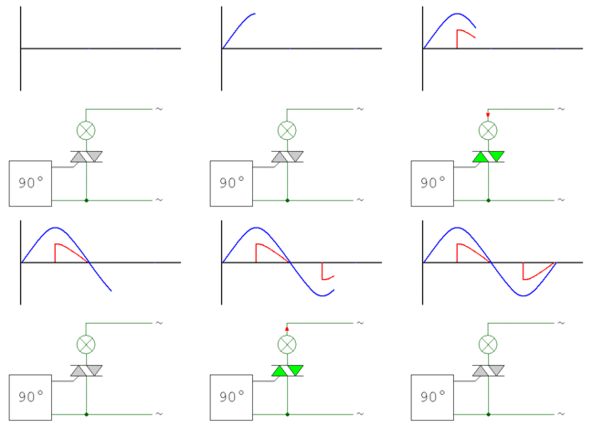
Low-power TRIACs are used in many applications such as light dimmers, speed controls for electric fans and other electric motors, and in the modern computerized control circuits of many household small and major appliances.
When mains voltage TRIACs are triggered by microcontrollers, optoisolators are frequently used; for example optotriacs can be used to control the gate current. Alternatively, where safety allows and electrical isolation of the controller isn't necessary, one of the microcontroller's power rails may be connected one of the mains supply. In these situations it is normal to connect the neutral terminal to the positive rail of the microcontroller's power supply, together with A1 of the triac, with A2 connected to the live. The TRIAC's gate can be connected through a resistor, and sometimes a transistor to the microcontroller, so that bringing the voltage down to the microcontroller's logic zero pulls enough current through the TRIAC's gate to trigger it. This ensures that the TRIAC is triggered in quadrants II and III and avoids quadrant IV where TRIACs are typically insensitive.[5]
Example data
| Variable name | Parameter | Typical value | Unit |
|---|---|---|---|
| Gate threshold voltage | 0.7-1.5 | V | |
| Gate threshold current | 5–50 | mA | |
| Repetitive peak off-state forward voltage | 600–800 | V | |
| Repetitive peak off-state reverse voltage | 600–800 | V | |
| RMS on-state current | 4–40 | A | |
| On-state current, non-repetitive peak | 100–270 | A | |
| On-state forward voltage | 1.5 | V |
Three-quadrant TRIAC
Three-quadrant TRIACs only operate in quadrants 1 through 3 and cannot be triggered in quadrant 4. These devices are made specifically for improved commutation and can often control reactive loads without the use of a snubber circuit.
The first TRIACs of this type were marketed by Thomson Semiconductors (now ST Microelectronics) under the name "Alternistor". Later versions are sold under the trademark "Snubberless". Littelfuse also uses the name "Alternistor". Phillips Semiconductor (now NXP Semiconductors) originated the trademark "High Commutation" ("Hi-Com").
Other three-quadrant TRIACs can operate with smaller gate-current to be directly driven by logic level components.
See also
- Thyristor
- Diode for alternating current (DIAC)
- Silicon-controlled rectifier (SCR)
- Quadrac
- Gate Turn-off Thyristor (GTO)
References
- 1 2 "Thyristor Theory and Design Considerations", ON Semiconductor, available at www.onsemi.com/pub/Collateral/HBD855-D.PDF
- 1 2 3 4 5 M.D. Singh, K.B. Khanchandani, Power Electronics, Second Edition, Tata McGraw-Hill, New Delhi, 2007, pages 148-152
- 1 2 Application Note AN-3008, RC Snubber Networks for Thyristor Power Control and Transient Suppression, Fairchild Semiconductor, available at http://www.fairchildsemi.com/an/AN/AN-3008.pdf, pages 1-5
- ↑ "2N6071A/B Series Sensitive Gate Triacs" (PDF). Semiconductor Components Industries, LLC. Retrieved June 28, 2012.
- ↑ triacs and microcontrollers - the easy connection
- ↑ "Philips Semiconductors Product specification Triacs BT138 series" (PDF). 090119 nxp.com
- ↑ "STMicroelectronics T3035H, T3050H Snubberless high temperature 30 A Triacs" (PDF). st.com 100922
Further reading
- Thyristor Theory and Design Considerations; ON Semiconductor; 240 pages; 2006; HBD855/D. (Free PDF download)
External links
| Wikimedia Commons has media related to Triacs. |
