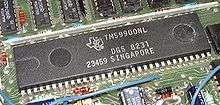
Texas Instruments TMS9900
| Designer | Texas Instruments |
|---|---|
| Bits | 16-bit |
| Introduced | 1976 |
| Design | CISC |
| Endianness | Big |
| Registers | |
| PC, WP, ST | |
| General purpose | 16 × 16-bit in external RAM |
Introduced in June 1976, the TMS9900 was one of the first commercially available, single-chip 16-bit microprocessors. The TMS9900 found its most widespread use in the TI-99/4 and TI-99/4A home computers.
History
The TMS9900 was designed as a single chip version of the TI 990 minicomputer series, much like the Intersil 6100 was a single chip PDP-8 (12 bit), and the Fairchild 9440 and Data General mN601 were both one-chip versions of Data General's Nova. Unlike other 16-bit microprocessors such as the National Semiconductor IMP-16 or DEC LSI-11, some of which predated the TMS9900, the latter was a single-chip, self-contained 16-bit microprocessor.
Architecture
The TMS9900 has three internal 16-bit registers — Program counter (PC), Status register (ST), and Workspace Pointer register (WP).[1] The WP register points to a base address in external RAM where the processor's 16 general purpose user registers (each 16 bits wide) are kept. This architecture allows for quick context switching; e.g. when a subroutine is entered, only the single workspace register needs to be changed instead of requiring registers to be saved individually.
Addresses refer to bytes with big endian ordering convention. The TMS9900 is a classic 16 bit machine with an address space of 216 bytes (65,536 bytes or 32,768 words).
There is no concept of a stack and no stack pointer register. Instead, Branch instructions exist that save the program counter to a register and change the register context. The 16 hardware and the 16 software interrupt vectors each consist of a pair of PC and WP values, so the register context switch is automatically performed by an interrupt as well.
Instruction set and addressing
The TMS9900 has 69 instructions which are one, two or three words long and always word-aligned in memory. The instruction set is fairly orthogonal, meaning that with few exceptions, instructions can use all methods of accessing operands (addressing modes).
Addressing modes include Immediate (operand in instruction), Direct or "Symbolic" (operand address in instruction), Register (operand in workspace register), Register Indirect (operand address in workspace register) with or without auto-increment, Indexed (operand address in instruction indexed with workspace register content), and Program Counter Relative.
The most important dual-operand instructions (add, subtract, compare, move etc.) contain 2-bit addressing mode and 4-bit register selector fields for both source and destination operands. In the opcode, "Symbolic" mode is represented as Indexed mode with the register field set to 0, therefore workspace register 0 (WR0) cannot be used in Indexed mode. In less frequently used dual-operand instructions like XOR, the destination operand must be a workspace register (or workspace register pair in the case of multiply and divide instructions).
Flow control is facilitated through a group of one unconditional and twelve conditional Jump instructions. Jump targets are relative to PC with an offset of -128 to +127 word addresses.
For subroutine calls, the Branch and Load Workspace Pointer (BLWP) instruction loads new WP and PC values, then saves the values of WP, PC and ST to the (new) registers 13, 14 and 15 respectively. At the end of the subroutine, the Return Workspace Pointer (RTWP) restores these in reverse order. Using BLWP/RTWP, it is possible to nest subroutine calls despite the absence of a stack, however, the programmer needs to assign the appropriate register workspace explicitly.
The instruction set also contains a Branch and Link (BL) opcode that only saves PC to register 11 without changing WP. In this case, a branch instruction (B) using WR11 as the destination address can serve as the return opcode, but BL-type subroutines cannot be nested without the programmer taking actions to save the return address.
The TMS9900 has an uncommon, and rarely used, instruction called "X" (eXecute). This instruction is used to execute another instruction at an address pointed to by a register without changing program flow, i.e. execution continues at the address following the X instruction. This instruction can be used for debugging (as a breakpoint instruction) and for creating indexed-opcode tables as used in byte-code interpreters.
The TMS9900 also supports the eXtended OPeration (XOP) instruction. XOP is given a number in the range 0-15 as well as a source address. When invoked, the instruction will perform a context switch through one of sixteen vectors at predefined locations in memory. This is similar to an interrupt, but the XOP instruction also stores the source address in register 11 of the new workspace. XOP is less flexible than a BLWP, as the transfer vectors have to be at fixed locations, but saves memory, since the source address can be used by the executed subroutine instead, when it's not defining the location of the vector. XOP is used to implement instructions in software in lower end models, where higher end versions of the 990 minicomputer series may have dedicated hardware to execute them.
In typical comparisons with the Intel 8086, the TMS9900 had smaller programs. The only disadvantage was the small address space and need for fast RAM.
Implementation

The TMS9900 was implemented in an N-channel silicon gate MOS process,[2] which required +5V, -5V and +12V power supplies and a four-phase (non-overlapping) clock with a maximum frequency of 3 MHz (333ns cycle),[3] usually generated from a 48 MHz crystal using a TIM9904 (aka 74LS362) clock generator chip.
The shortest instructions require eight clock cycles or 2.7 μs to complete (assuming 0 external wait cycles), many others run between 10 and 14 cycles (3.3-4.7 μs); the longest-running instruction (DIV) can take up to 124 cycles (41.3 μs).[4]
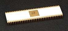
The chip was packaged in a (then unusual) 64-pin, 0.9" wide DIP. The comparatively large number of pins allowed for the 15-bit (word) address bus and 16-bit data bus to be brought out on dedicated pins without the use of multiplexing (unlike e.g. the Intel 8086 CPU), keeping external memory connections simple. Contrary to the convention used by many other manufacturers, TI labeled the most significant address and data lines "A0" and "D0", respectively. All internal data paths and the ALU are 16 bits wide.
The processor can be paused with the address bus tri-stated for external direct memory access (DMA). Memory accesses are always 16 bits wide, with the CPU automatically performing read-before-write operations for byte-wide accesses.
The hardware interrupt system supports a 4-bit interrupt priority input, which needed to be higher than the priority level stored in the status register (bits 12-15) in order for the interrupt request to be served. In addition, the /LOAD input provides a non-maskable interrupt facility with a dedicated vector.[5]
The TMS9900 CPU also contains a 16-bit shift register ("CRU") designed for interfacing with external shift registers, with dedicated instructions supporting access to fields of 1-16 bit width out of a total of 4096 addressable bits.
Parallel peripherals can be attached in memory-mapped fashion to the regular address and data bus.
Applications
The TMS9900 was used in the TI-99/4 and TI-99/4A home computers. Unfortunately, to reduce the production costs, TI chose to use in these systems just 128 16-bit words of the fast kind of RAM that the TMS9900 could access directly. The rest of the memory was 16kB of 8-bit DRAM that was accessible only indirectly through the video display controller, which crippled the performance of the TI-99/4.
TI developed the TM990 series of computer modules, including CPU, memory, I/O, which when plugged into a card frame could form a 16-bit minicomputer. These were typically used for process control.[6] A microprocessor trainer was released in the form of the TM990/189.[7]
TMS9900 Family Product Development
The second generation of the TMS9900 family of microprocessors took the form of the TMS9995. This provided "functional performance at speeds 3 times faster than any previous 9900 family processor",[8] largely due to the inclusion of instruction prefetch technology. In the home computer arena, the TMS9995 was used in the TI-99/2 & TI-99/8 prototypes, the Myarc Geneve 9640, the Tomy Tutor, and the Powertran Cortex.[9]
TI later developed the more powerful and more capable TMS99000 family of microprocessors, which was used as the CPU in the 990/10A minicomputer as a cost reduction. Unfortunately, by the time the 990/10A made it to market, the end of the minicomputer era was already in sight.
The TMS99000 family includes two microprocessors,[10] the TMS99105A and the TMS99110A, which are identical except for specialized pre-programming of the on-chip Macrostore ROM memory (Macrostore memory space implements added functions or instructions through emulation routines written in standard machine code). The on-chip ROM Macrostore in the TMS99105A microprocessor is not utilized. The on-chip ROM Macrostore in the TMS99110A microprocessor contains floating point instructions which are available as part of the machine language instruction set. A third member of the TMS99000 family, the TMS99120, was announced[11] but may never have been commercially produced. The on-chip ROM Macrostore in the TMS99120 contains run-time support routines for the PASCAL high-level language.
Variants
| Model | Description |
|---|---|
| TI990/9 | Early multi-chip CPU for minicomputer systems, 1974 |
| TI990/10 | Multi-chip implementation for minicomputer systems, 1975 |
| TI990/12 | Multi-chip implementation, faster than 990/10. |
| TMS9900 | Single chip implementation, 1976. Used in the TI-99/4(A) computer. |
| TMS9940 | Microcontroller with 2KB ROM, 128B RAM, decrementer, CRU bus, 1979 |
| TMS9980, TMS9981 | 8-bit versions of TMS9900 |
| TMS9985 | A TMS9940 with 8KB ROM, 256B RAM, and an 8-bit external bus, c. 1978 (never released) |
| TMS9989 | Improved 9980, used in military hardware. |
| TMS9995 | Improved TMS9985-like, no ROM. Used in the TI-99/2 & TI-99/8 prototypes, the Tomy Tutor and the Geneve computer. |
| TMS99105 | Baseline member of the TMS99000 microprocessor family. |
| TMS99110 | TMS99000 family microprocessor with floating point instructions pre-programmed into the on-chip Macrostore ROM memory. |
| TMS99120 | TMS99000 family microprocessor with run-time support routines for the PASCAL high-level language pre-programmed into the on-chip Macrostore ROM memory. (Microprocessor was announced but may never have been commercially produced.) |
- Die photos
 TMS9900
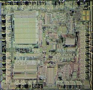 TMS9981
 TMS9995
 TMS99105A
References
- ↑ TMS9900 Microprocessor Data Manual (PDF). Texas Instruments Inc. 1976. p. 3.
- ↑ TMS9900 Microprocessor Data Manual (PDF). Texas Instruments Inc. 1976. p. 3.
- ↑ TMS9900 Microprocessor Data Manual (PDF). Texas Instruments Inc. 1976. p. 31.
- ↑ TMS9900 Microprocessor Data Manual (PDF). Texas Instruments Inc. 1976. p. 28.
- ↑ TMS9900 Microprocessor Data Manual (PDF). Texas Instruments Inc. 1976. p. 6.
- ↑ "Stuart's TM 990 Series 16-Bit Microcomputer Modules". Retrieved 2014-03-25.
- ↑ "Programmable Calculators - Texas Instruments TM990/189". Retrieved 2014-03-25.
- ↑ TMS9995 marketing brochure (PDF). Texas Instruments Inc. 1981. p. 2.
- ↑ "Powertran Cortex.com". Retrieved 2014-03-27.
- ↑ TMS99105A and TMS99110A 16-Bit Microprocessors Preliminary Data Manual (PDF). Texas Instruments Inc. 1982. p. 1.
- ↑ Microsystems Designers Handbook, 2nd Edition. Texas Instruments Limited. 1981. pp. 3–25 onwards.
External links
- TMS9900 manuals and references from Bitsavers