Transition metal dichalcogenide monolayers
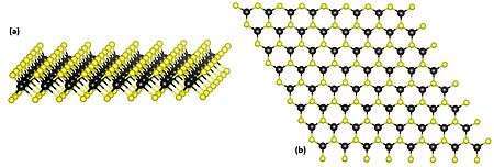
Transition metal dichalcogenide (TMDC) monolayers are atomically thin semiconductors of the type MX2, with M a transition metal atom (Mo, W, etc.) and X a chalcogen atom (S, Se, or Te.). One layer of M atoms is sandwiched between two layers of X atoms. A MoS2 monolayer is 6.5 Å thick.
The discovery of graphene shows how new physical properties emerge when a bulk crystal of macroscopic dimensions is thinned down to one atomic layer. Like graphite, TMDC bulk crystals are formed of monolayers bound to each other by Van-der-Waals attraction. TMDC monolayers have properties that are distinctly different from those of the semimetal graphene:
- TMDC monolayers MoS2, WS2, MoSe2, WSe2, MoTe2 have a direct band gap, and can be used in electronics as transistors and in optics as emitters and detectors.[1][2][3][4][5]
- The TMDC monolayer crystal structure has no inversion center, which allows to access a new degree of freedom of charge carriers, namely the k-valley index, and to open up a new field of physics: valleytronics[6][7][8][9]
- The strong spin-orbit coupling in TMDC monolayers leads to a spin-orbit splitting [10] of hundreds meV in the valence band and a few meV in the conduction band, which allows control of the electron spin by tuning the excitation laser photon energy.
The work on TMDC monolayers is an emerging research and development field since the discovery of the direct bandgap[1][2] and the potential applications in electronics[3] and valley physics.[7][8][9] TMDCs are often combined with other 2d materials like graphene and hexagonal boron nitride to make van der Waals heterostructure devices.
Crystal structure
In the macroscopic bulk crystal, or more precisely, for an even number of monolayers, the crystal structure has an inversion center. In the case of a monolayer (or any odd number of layers), the crystal has no inversion center. Two important consequences of that are:
- nonlinear optical phenomena, such as second-harmonic generation. When the crystal is excited by a laser, the output frequency can be doubled.[11][12][13][14]
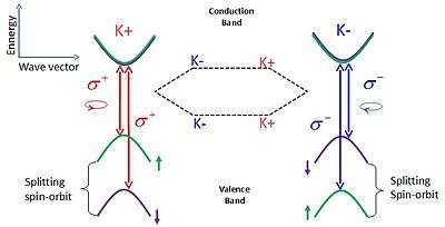
- an electronic band structure with direct energy gaps, where both conduction and valence band edges are located at the non-equivalent K points (K+ and K-) of the 2D hexagonal Brillouin zone. The interband transitions in the vicinity of the K+ (or K-) point are coupled to right (or left) circular photon polarization states. These so-called valley dependent optical selection rules arise from inversion symmetry breaking. This provides a convenient method to address specific valley states (K+ or K-) by circularly polarized (right or left) optical excitation.[9] In combination with strong spin-splitting, the spin and valley degree of freedom are coupled, enabling stable valley polarization.[15][16][17]
These properties indicate that TMDC monolayers represent a promising platform to explore spin and valley physics with the corresponding possible applications.
Properties
Transport properties
At submicron scales, 3D materials no longer have the same behavior as their 2D form, which can be an advantage. For example, graphene has a very high carrier mobility, and accompanying lower losses through the Joule effect. But graphene has zero bandgap, which results in a disqualifying low on/off ratio in transistor applications. TMDC monolayers might be an alternative: they are structurally stable, display a band gap and show electron mobilities comparable to those of silicon, so they can be used to fabricate transistors.
In 2004, the first field-effect transistor (FET) made of bulk WSe2 was reported. It showed a mobility below 500 cm2 V−1 s−1 for p-type conductivity at room temperature, about half that of a silicon FET but a low on/off current ratio because the device was realised on the surface of a bulk crystal. FETs made of monolayer MoS2 showed an excellent on/off ratio exceeding 108.[3]
High carrier mobility, high on/off ratio and small thickness (one monolayer) of TMDC devices are potentially interesting for such applications.
Optical properties
| A (eV) | A (nm) | B (eV) | B (nm) | |
|---|---|---|---|---|
| MoS2 | 1.78 | 695 | 1.96 | 632 |
| MoSe2 | 1.50 | 825 | 1.75 | 708 |
| MoTe2 | ||||
| WS2 | 1.84 | 673 | 2.28 | 544 |
| WSe2 | 1.52 | 815 | 2.00 | 619 |
A semiconductor can absorb photons with energy larger than or equal to its bandgap. This means that light with a shorter wavelength is absorbed. Semiconductors are typically efficient emitters if the minimum of the conduction band energy is at the same position in k-space as the maximum of the valence band, i.e., the band gap is direct. The band gap of bulk TMDC material down to a thickness of two monolayers is still indirect, so the emission efficiency is lower compared to monolayered materials. The emission efficiency is about 104 greater for TMDC monolayer than for bulk material.[4] The band gaps of TMDC monolayers are in the visible range (between 400 nm and 700 nm). The direct emission shows two transitions called A and B, separated by the spin-orbit coupling energy. The lowest energy and therefore most important in intensity is the A emission.[1][19] Owing to their direct band gap, TMDC monolayers are promising materials for optoelectronics applications.
.jpg)
Atomic layers of MoS2 have been used as a phototransistor and ultrasensitive detectors. Phototransistors are important devices: the first with a MoS2 monolayer active region shows a photoresponsivity of 7.5 mA W−1 which is similar to graphene devices that reach 6.1 mA W−1. Multilayer MoS2 show higher photoresponsivities, about 100 mA W−1, which is similar to silicon devices. Making a gold contact at the far edges of a monolayer allows an ultrasensitive detector to be fabricated.[5] Such a detector has a photoresponsivity reaching 880 A W−1, 106 greater than the first graphene photodetectors. This high degree of electrostatic control is due to the thin active region of the monolayer. Its simplicity and the fact that it has only one semiconductor region, whereas the current generation of photodetectors is typically a p-n junction, makes possible industrial applications such as high-sensitivity and flexible photodetectors. The only limitation for currently available devices is the slow photoresponse dynamics.[5]
Mechanical properties
A monolayer of MoS2 can be strained at least up to 10%,[20] comparable to graphene. Under the application of strain, a decrease in the direct and indirect band gap is measured that is approximately linear with strain.[21] Importantly, the indirect bandgap increases faster with applied strain to the monolayer than the direct bandgap, resulting in a crossover from direct to indirect band gap at a strain level of around 1%.[22] As a result, the emission efficiency of monolayers is expected to decrease for highly strained samples.[23] This property allows mechanical tuning of the electronic structure and also the possibility of fabrication of flexible electronics i.e. on flexible substrates.
Fabrication of TMDC monolayers
Exfoliation
Exfoliation is a top down approach. In the bulk form, TMDCs are crystals made of layers, which are coupled by Van-der-Waals forces. These interactions are weaker than the chemical bonds between the Mo and S in MoS2, for example. So TMDC monolayers can be produced by micromechanical cleavage, just as graphene.
The crystal of TMDC is rubbed against the surface of another material (any solid surface). In practice, adhesive tape is placed on the TMDC bulk material and subsequently removed. The adhesive tape, with tiny TMDC flakes coming off the bulk material, is brought down onto a substrate. On removing the adhesive tape from the substrate, TMDC monolayer and multilayer flakes are deposited. This technique produces small samples of monolayer material, typically about 5–10 micrometers in diameter.[24]
Large quantities of exfoliated material can also be produced using liquid-phase exfoliation by blending TMDC materials with solvents and polymers. [25]
Chemical vapor deposition
Chemical vapor deposition is a bottom-up approach. For example, the synthesis of MoS2 is made using: SiO2 as a substrate, MoO3 and S powders used as reactants. The reactants are delivered on the substrate and the whole is heated to 650 Celsius degrees in the presence of N2. The size of the sample is larger than obtained with the exfolation technique.[26]
Molecular beam epitaxy
Molecular beam epitaxy (MBE) is an established technique for growing semiconductor devices with atomic monolayer thickness control. As a promising demonstration, high-quality monolayer MoSe2 samples have been grown on graphene by MBE.[27]
Electronic band structure
Band gap
In the bulk form, TMDC have an indirect gap in the center of the Brillouin zone, whereas in monolayer form the gap becomes direct and is located in the K point.[2][1]
Spin-orbit coupling
| Valence band
splitting (eV) |
Conduction band
splitting (eV) | |
|---|---|---|
| MoS2 | 0.148 | 0.003 |
| WS2 | 0.430 | 0.026 |
| MoSe2 | 0.184 | 0.007 |
| WSe2 | 0.466 | 0.038 |
| MoTe2 | 0.219 | 0.034 |
For TMDCs, the atoms are heavy and the outer layers electronic states are from d-orbitals that have a strong spin-orbit coupling. This spin orbit coupling removes the spins degeneracy in both the conduction and valence band i.e. introduces a strong energy splitting between spin up and down states. In the case of MoS2, the spin splitting in conduction band is in the meV range, it is expected to be more pronounced in other material like WS2.[30][31][32] The spin orbit splitting in the valence band is several hundred meV.
Spin-valley coupling and the electron valley degree of freedom
By controlling the charge or spin degree of freedom of carriers, as proposed by spintronics, novel devices have already been made. If there are different conduction/valence band extrema in the electronic band structure in k-space, the carrier can be confined in one of these valleys. This degree of freedom opens up a new field of physics: the controlling of carriers k-valley index, also called valleytronics.[15]
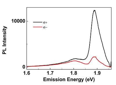
For TMDC monolayers crystals, the parity symmetry is broken, there is no more inversion center. K valleys of different directions in the 2D hexagonal Brillouin zone are no longer equivalent. So there are two kinds of K valley call K+ and K-. Also there is a strong energy degeneracy of different spin states in valence band. The transformation of one valley to another is described by the time reversal operator. Moreover, crystal symmetry leads to valley dependent optical selection rules: a right circular polarized photon (σ+) initialize a carrier in the K+ valley and a left circular polarized photon (σ-) initialize a carrier in the K- valley.[7] Thanks to these two properties (spin-valley coupling and optical selection rules), a laser of specific polarization and energy allows to initialize the electron valley states (K+ or K-) and spin states (up or down).
Emission and absorption of light: excitons
A single layer of TMDC can absorb 5-10% of light,[33] which is unprecedented for such a thin material. When a photon of suitable energy is absorbed by a TMDC monolayer, an electron is created in the conduction band; the electron now missing in the valence band is assimilated by a positively charged quasi-particle called a hole. The negatively charged electron and the positively charged hole are attracted via the Coulomb interaction, forming a bound state called an exciton. This results in an important energy difference between the bandgap observed in optical experiments ('optical bandgap') and the true bandgap for free carrier absorption. This is referred to as bandgap renormalization and occurs, albeit on smaller energy scales, in semiconductors like GaAs and ZnO. The energy difference between the optical bandgap and the free carrier bandgap is called the exciton binding energy. In atomically thin 2D systems there exists a strong confinement of electrons and holes in the layer plane.[19] This confinement dramatically enhances the Coulomb interaction between the electron and hole in TMDC monolayers compared to the bulk situation or other quasi 2D materials, leading to a large binding energy in the hundreds of meV range.[14][19][34][35][36]
Trions (charged excitons)[37][38] and biexcitons[39][40] have been observed in monolayer transition-metal dichalcogenides.
References
- 1 2 3 4 Splendiani, A.; Sun, L.; Zhang, Y.; Li, T.; Kim, J.; Chim, C. Y.; Galli, G.; Wang, F. (2010). "Emerging Photoluminescence in Monolayer MoS2". Nano Letters. 10 (4): 1271–5. doi:10.1021/nl903868w. PMID 20229981.
- 1 2 3 Mak, K. F.; Lee, C.; Hone, J.; Shan, J.; Heinz, T. F. (2010). "Atomically Thin MoS2: A New Direct-Gap Semiconductor". Physical Review Letters. 105 (13). arXiv:1004.0546
 . doi:10.1103/PhysRevLett.105.136805.
 - 1 2 3 4 Radisavljevic, B.; Radenovic, A.; Brivio, J.; Giacometti, V.; Kis, A. (2011). "Single-layer MoS2 transistors". Nature Nanotechnology. 6 (3): 147–50. doi:10.1038/nnano.2010.279. PMID 21278752.
- 1 2 Sundaram, R. S.; Engel, M.; Lombardo, A.; Krupke, R.; Ferrari, A. C.; Avouris, Ph; Steiner, M. (2013). "Electroluminescence in Single Layer MoS2". Nano Letters. 13 (4): 1416–1421. doi:10.1021/nl400516a. ISSN 1530-6984.
- 1 2 3 4 Lopez-Sanchez, O.; Lembke, D.; Kayci, M.; Radenovic, A.; Kis, A. (2013). "Ultrasensitive photodetectors based on monolayer MoS2". Nature Nanotechnology. 8 (7): 497–501. doi:10.1038/nnano.2013.100. PMID 23748194.
- ↑ Rycerz, A.; Tworzydło, J.; Beenakker, C. W. J. (2007). "Valley filter and valley valve in graphene". Nature Physics. 3 (3): 172. arXiv:cond-mat/0608533. doi:10.1038/nphys547.
- 1 2 3 Cao, T.; Wang, G.; Han, W.; Ye, H.; Zhu, C.; Shi, J.; Niu, Q.; Tan, P.; Wang, E.; Liu, B.; Feng, J. (2012). "Valley-selective circular dichroism of monolayer molybdenum disulphide". Nature Communications. 3 (6): 887. doi:10.1038/ncomms1882. PMC 3621397. PMID 22673914.
- 1 2 Mak, K. F.; He, K.; Shan, J.; Heinz, T. F. (2012). "Control of valley polarization in monolayer MoS2 by optical helicity". Nature Nanotechnology. 7 (8): 494–8. doi:10.1038/nnano.2012.96. PMID 22706698.
- 1 2 3 Zeng, H.; Dai, J.; Yao, W.; Xiao, D.; Cui, X. (2012). "Valley polarization in MoS2 monolayers by optical pumping". Nature Nanotechnology. 7 (8): 490–3. arXiv:1202.1592. doi:10.1038/nnano.2012.95. PMID 22706701.
- ↑ Reyes-Retana, J.A.; Cervantes-Sodi, F. (2016). "Spin-orbital effects in metal-dichalcogenide semiconducting monolayers". Scientific Reports. 6. doi:10.1038/srep24093.
- ↑ Kumar, N.; Najmaei, S.; Cui, Q.; Ceballos, F.; Ajayan, P.; Lou, J.; Zhao, H. (2013). "Second harmonic microscopy of monolayer MoS2". Physical Review B. 87 (16). arXiv:1302.3935v2. doi:10.1103/PhysRevB.87.161403.
- ↑ Malard, L. M.; Alencar, T. V.; Barboza, A. P. M.; Mak, K. F.; De Paula, A. M. (2013). "Observation of intense second harmonic generation from MoS2 atomic crystals". Physical Review B. 87 (20). arXiv:1304.4289. doi:10.1103/PhysRevB.87.201401.
- ↑ Zeng, H.; Liu, G. B.; Dai, J.; Yan, Y.; Zhu, B.; He, R.; Xie, L.; Xu, S.; Chen, X.; Yao, W.; Cui, X. (2013). "Optical signature of symmetry variations and spin-valley coupling in atomically thin tungsten dichalcogenides". Scientific Reports. 3. arXiv:1208.5864. doi:10.1038/srep01608.
- 1 2 Wang, G.; et al. (2014). "Non-linear Optical Spectroscopy of Excited Exciton States for Efficient Valley Coherence Generation in WSe2 Monolayers". arXiv:1404.0056.
- 1 2 Xiao, D.; Liu, G. B.; Feng, W.; Xu, X.; Yao, W. (2012). "Coupled Spin and Valley Physics in Monolayers of MoS2 and Other Group-VI Dichalcogenides". Physical Review Letters. 108 (19). doi:10.1103/PhysRevLett.108.196802.
- ↑ Jones, A. M.; Yu, H.; Ghimire, N. J.; Wu, S.; Aivazian, G.; Ross, J. S.; Zhao, B.; Yan, J.; Mandrus, D. G.; Xiao, D.; Yao, W.; Xu, X. (2013). "Optical generation of excitonic valley coherence in monolayer WSe2". Nature Nanotechnology. 8 (9): 634–8. arXiv:1303.5318. doi:10.1038/nnano.2013.151. PMID 23934096.
- ↑ Xu, X.; Yao, W.; Xiao, D.; Heinz, T. F. (2014). "Spin and pseudospins in layered transition metal dichalcogenides". Nature Physics. 10 (5): 343. doi:10.1038/nphys2942.
- ↑ Ramasubramaniam, A. (2012). "Large excitonic effects in monolayers of molybdenum and tungsten dichalcogenides". Physical Review B. 86 (11). doi:10.1103/PhysRevB.86.115409.
- 1 2 3 Qiu, D. Y.; Da Jornada, F. H.; Louie, S. G. (2013). "Optical Spectrum of MoS2: Many-Body Effects and Diversity of Exciton States". Physical Review Letters. 111 (21). arXiv:1311.0963. doi:10.1103/PhysRevLett.111.216805.
- ↑ Bertolazzi, Simone; Brivio, Jacopo; Kis, Andras (2011). "Stretching and Breaking of Ultrathin MoS2". ACS Nano. 5 (12): 9703–9709. doi:10.1021/nn203879f.
- ↑ He, K.; Poole, C.; Mak, K. F.; Shan, J. (2013). "Experimental Demonstration of Continuous Electronic Structure Tuning via Strain in Atomically Thin MoS2". Nano Letters. 13 (6): 2931–6. arXiv:1305.3673. doi:10.1021/nl4013166. PMID 23675872.
- ↑ Conley, H. J.; Wang, B.; Ziegler, J. I.; Haglund, R. F.; Pantelides, S. T.; Bolotin, K. I. (2013). "Bandgap Engineering of Strained Monolayer and Bilayer MoS2". Nano Letters. 13 (8): 3626–30. arXiv:1305.3880. doi:10.1021/nl4014748. PMID 23819588.
- ↑ Zhu, C. R.; Wang, G.; Liu, B. L.; Marie, X.; Qiao, X. F.; Zhang, X.; Wu, X. X.; Fan, H.; Tan, P. H.; Amand, T.; Urbaszek, B. (2013). "Strain tuning of optical emission energy and polarization in monolayer and bilayer MoS2". Physical Review B. 88 (12). arXiv:1306.3442. doi:10.1103/PhysRevB.88.121301.
- ↑ Novoselov, K. S.; Jiang, D; Schedin, F; Booth, T. J.; Khotkevich, V. V.; Morozov, S. V.; Geim, A. K. (2005). "Two-dimensional atomic crystals". Proceedings of the National Academy of Sciences. 102 (30): 10451–3. doi:10.1073/pnas.0502848102. PMC 1180777. PMID 16027370.
- ↑ Coleman, Jonathan N.; Lotya, Mustafa; O’Neill, Arlene; Bergin, Shane D.; King, Paul J.; Khan, Umar; Young, Karen; Gaucher, Alexandre; De, Sukanta; Smith, Ronan J.; Shvets, Igor V.; Arora, Sunil K.; Stanton, George; Kim, Hye-Young; Lee, Kangho; Kim, Gyu Tae; Duesberg, Georg S.; Hallam, Toby; Boland, John J.; Wang, Jing Jing; Donegan, John F.; Grunlan, Jaime C.; Moriarty, Gregory; Shmeliov, Aleksey; Nicholls, Rebecca J.; Perkins, James M.; Grieveson, Eleanor M.; Theuwissen, Koenraad; McComb, David W.; Nellist, Peter D.; Nicolosi, Valeria (2011-02-04). "Two-Dimensional Nanosheets Produced by Liquid Exfoliation of Layered Materials". Science. 331 (6017): 568–571. doi:10.1126/science.1194975.
- ↑ Lee, Y. H.; Zhang, X. Q.; Zhang, W; Chang, M. T.; Lin, C. T.; Chang, K. D.; Yu, Y. C.; Wang, J. T.; Chang, C. S.; Li, L. J.; Lin, T. W. (2012). "Synthesis of large-area MoS2 atomic layers with chemical vapor deposition". Advanced Materials. 24 (17): 2320–5. arXiv:1202.5458. doi:10.1002/adma.201104798. PMID 22467187.
- ↑ Zhang, Y.; Chang, T. R.; Zhou, B.; Cui, Y. T.; Yan, H.; Liu, Z.; Schmitt, F.; Lee, J.; Moore, R.; Chen, Y.; Lin, H.; Jeng, H. T.; Mo, S. K.; Hussain, Z.; Bansil, A.; Shen, Z. X. (2013). "Direct observation of the transition from indirect to direct bandgap in atomically thin epitaxial MoSe2". Nature Nanotechnology. 9 (2): 111–5. arXiv:1401.3386. doi:10.1038/nnano.2013.277. PMID 24362235.
- ↑ Cheng, Y. C.; Zhu, Z. Y.; Tahir, M.; Schwingenschlogl, U. (2012). "Spin-orbit–induced spin splittings in polar transition metal dichalcogenide monolayers". EPL(Europhysics Letters). 102 (5): 57001. doi:10.1209/0295-5075/102/57001.
- 1 2 Liu, G. B.; Shan, W. Y.; Yao, Y.; Yao, W.; Xiao, D. (2013). "Three-band tight-binding model for monolayers of group-VIB transition metal dichalcogenides". Physical Review B. 88 (8). arXiv:1305.6089. doi:10.1103/PhysRevB.88.085433.
- ↑ Zhu, Z.; Cheng, Y. C.; Schwingenschlogl, U. (2011). "Giant spin-orbit-induced spin splitting in two-dimensional transition-metal dichalcogenide semiconductors". Physical Review B. 84 (15): 153402. doi:10.1103/PhysRevB.84.153402.
- ↑ Kośmider, K.; González, J. W.; Fernández-Rossier, J. (2013). "Large spin splitting in the conduction band of transition metal dichalcogenide monolayers". Physical Review B. 88 (24). doi:10.1103/PhysRevB.88.245436.
- ↑ Kormányos, A.; Zólyomi, V.; Drummond, N. D.; Burkard, G. (2014). "Spin-Orbit Coupling, Quantum Dots, and Qubits in Monolayer Transition Metal Dichalcogenides". Physical Review X. 4. arXiv:1310.7720. doi:10.1103/PhysRevX.4.011034.
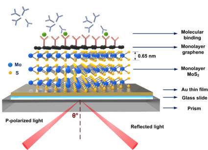
- 1 2 Zeng, Shuwen; Hu, Siyi; Xia, Jing; Anderson, Tommy; Dinh, Xuan-Quyen; Meng, Xiang-Min; Coquet, Philippe; Yong, Ken-Tye (2015). "Graphene–MoS2 Hybrid Nanostructures enhanced Surface Plasmon Resonance Biosensors". Sensors and Actuators B: Chemical. doi:10.1016/j.snb.2014.10.124.
- ↑ Chernikov, Alexey; Berkelbach, Timothy C.; Hill, Heather M.; Rigosi, Albert; Li, Yilei; Aslan, Ozgur Burak; Reichman, David R.; Hybertsen, Mark S.; Heinz, Tony F. (2014). "Exciton Binding Energy and Nonhydrogenic Rydberg Series in Monolayer WS2". Physical Review Letters. 113 (7). arXiv:1403.4270. doi:10.1103/PhysRevLett.113.076802.
- ↑ Ye, Ziliang; Cao, Ting; O’Brien, Kevin; Zhu, Hanyu; Yin, Xiaobo; Wang, Yuan; Louie, Steven G.; Zhang, Xiang (2014). "Probing excitonic dark states in single-layer tungsten disulphide". Nature. 513 (7517): 214–218. arXiv:1403.5568. doi:10.1038/nature13734. PMID 25162523.
- ↑ Ugeda, M. M.; Bradley, A. J.; Shi, S. F.; Da Jornada, F. H.; Zhang, Y.; Qiu, D. Y.; Ruan, W.; Mo, S. K.; Hussain, Z.; Shen, Z. X.; Wang, F.; Louie, S. G.; Crommie, M. F. (2014). "Giant bandgap renormalization and excitonic effects in a monolayer transition metal dichalcogenide semiconductor". Nature Materials. doi:10.1038/nmat4061.
- ↑ J. S. Ross; et al. (2013). "Electrical control of neutral and charged excitons in a monolayer semiconductor". Nat. Comm. 4: 1474. doi:10.1038/ncomms2498.
- ↑ K. F. Mak; et al. (2013). "Tightly bound trions in monolayer MoS2". Nat. Mater. 12: 207–211. doi:10.1038/nmat3505.
- ↑ C. Mai; et al. (2014). "Many-Body Effects in Valleytronics: Direct Measurement of Valley Lifetimes in Single-Layer MoS2". Nano Lett. 14: 202–206. doi:10.1021/nl403742j.
- ↑ J. Shang; et al. (2015). "Observation of Excitonic Fine Structure in a 2D Transition-Metal Dichalcogenide Semiconductor". ACS Nano. 9: 647–655. doi:10.1021/nn5059908.