Conductive atomic force microscopy
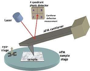
Conductive atomic force microscopy (C-AFM) is a variation of atomic force microscopy (AFM) and scanning tunneling microscopy (STM), which uses electrical current to construct the surface profile of the studied sample. The current is flowing through the metal-coated tip of the microscope and the conducting sample. Usual AFM topography, obtained by vibrating the tip, is acquired simultaneously with the current. This enables to correlate a spatial feature on the sample with its conductivity, and distinguishes C-AFM from STM where only current is recorded. A C-AFM microscope uses conventional silicon tips coated with a metal or metallic alloy, such as Pt-Ir alloy.[1]
The C-AFM can be operated in the imaging mode and spectroscopic mode.
Imaging mode
In the conventional imaging mode, vibrating tip is scanned over a small sample area (typically square micrometres); a negative voltage bias is applied to the sample, and the electrons tunneling from the sample to the tip are being collected. This polarity is chosen for several reasons: The electron barrier in this case is the conduction band onset at the Si/oxide interface, which is better known than the tip/oxide interface. The emission area for substrate injection is homogeneous and depends mostly on the tip/sample contact area. On the contrary, the emission area in the case of tip injection depends on the shape of the tip. During the measurement, the tip is in contact with the sample, and many studies materials are hydrophilic. Therefore, the tip drags along water and other contaminants adsorbed at the sample surface. The applied voltage induces a high electrical field between the tip and the substrate. This field ionizes water, producing the OH−. If a negative voltage is applied to the tip, the OH− ions are attracted to the surface of the sample; they oxidize it thereby permanently blocking the current flow. If a positive voltage is applied to the tip, the OH− ions are dragged to the tip, oxidizing it and breaking the electrical circuit. However, whereas the studied sample may be unique, the tips are disposable and easy to replace, but after replacement, it is difficult to relocate exactly the same area. The tip degradation, as well as image quality, also depend on the scanning parameters.[1]
Spectroscopic mode
In the spectroscopic mode, the tip is stationary, while the voltage is being swept. This allows recording conventional current–voltage characteristic from tiny areas of the sample, and thereby to extract information on the local electronic properties, such as local density of states.[1]
See also
- Microscopy
- Scanning probe microscopy
- Scanning tunneling spectroscopy
- Spin polarized scanning tunneling microscopy
References
- 1 2 3 Zhang, L.; T. Sakai; N. Sakuma; T. Ono; K. Nakayama (1999). "Nanostructural conductivity and surface-potential study of low-field-emission carbon films with conductive scanning probe microscopy". Applied Physics Letters. 75 (22): 3527–3529. Bibcode:1999ApPhL..75.3527Z. doi:10.1063/1.125377.
External links
| Wikibooks has a book on the topic of: The Opensource Handbook of Nanoscience and Nanotechnology |
| Wikimedia Commons has media related to Scanning tunneling microscope. |