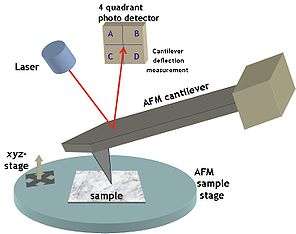
Atomic-force microscopy
Atomic-force microscopy (AFM) or scanning-force Microscopy (SFM) is a very-high-resolution type of scanning probe microscopy (SPM), with demonstrated resolution on the order of fractions of a nanometer, more than 1000 times better than the optical diffraction limit.
Overview

Atomic-force microscopy (AFM) or scanning-force microscopy (SFM) is a type of scanning probe microscopy (SPM), with demonstrated resolution on the order of fractions of a nanometer, more than 1000 times better than the optical diffraction limit. The information is gathered by "feeling" or "touching" the surface with a mechanical probe. Piezoelectric elements that facilitate tiny but accurate and precise movements on (electronic) command enable very precise scanning.
Abilities
The AFM has three major abilities: force measurement, imaging, and manipulation.
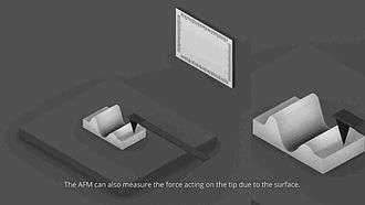
In force measurement, AFMs can be used to measure the forces between the probe and the sample as a function of their mutual separation. This can be applied to perform force spectroscopy.
For imaging, the reaction of the probe to the forces that the sample imposes on it can be used to form an image of the three-dimensional shape (topography) of a sample surface at a high resolution. This is achieved by raster scanning the position of the sample with respect to the tip and recording the height of the probe that corresponds to a constant probe-sample interaction (see section topographic imaging in AFM for more details). The surface topography is commonly displayed as a pseudocolor plot. An AFM image is a simulated image based on the height of each point of the surface and, in fact, each point (x, y) of the surface has a height h(x, y).[1]
In manipulation, the forces between tip and sample can also be used to change the properties of the sample in a controlled way. Examples of this include atomic manipulation, scanning probe lithography and local stimulation of cells.
Simultaneous with the acquisition of topographical images, other properties of the sample can be measured locally and displayed as an image, often with similarly high resolution. Examples of such properties are mechanical properties like stiffness or adhesion strength and electrical properties such as conductivity or surface potential. In fact, the majority of SPM techniques are extensions of AFM that use this modality.
Other microscopy technologies
Compared to competitive technologies such as optical microscopy and electron microscopy, the major difference between these and the atomic-force microscope is that the latter does not use lenses or beam irradiation. Therefore, it does not suffer from a limitation of space resolution due to diffraction limit and aberration, and it is not necessary to prepare a space for guiding the beam (by creating a vacuum) or to stain the sample.
There are several types of scanning microscopy including scanning probe microscopy (which includes AFM, STM and near-field scanning optical microscope (SNOM/NSOM), STED microscopy (STED), and scanning electron microscopy). Although SNOM and STED use visible light to illuminate the sample, their resolution is not constrained by the diffraction limit.
Configuration
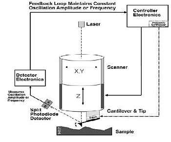
Fig. 3 shows an AFM typically consisting of the following features:[2]
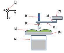
(1):: Cantilever, (2): Support for cantilever, (3): Piezoelectric element(to oscillate cantilever at its eigen frequency.), (4): Tip (Fixed to open end of a cantilever, acts as the probe), (5): Detector of deflection and motion of the cantilever, (6): Sample to be measured by AFM, (7): xyz drive, (moves sample (6) and stage (8) in x, y, and z directions with respect to a tip apex (4)), and (8): Stage.
The small spring-like cantilever (1) is carried by the support (2). Optionally, a piezoelectric element (3) oscillates the cantilever (1). The sharp tip (4) is fixed to the free end of the cantilever (1). The detector (5) records the deflection and motion of the cantilever (1). The sample (6) is mounted on the sample stage (8). An xyz drive (7) permits to displace the sample (6) and the sample stage (8) in x, y, and z directions with respect to the tip apex (4). Although Fig. 3 shows the drive attached to the sample, the drive can also be attached to the tip, or independent drives can be attached to both, since it is the relative displacement of the sample and tip that needs to be controlled. Controllers and plotter are not shown in Fig. 3. Numbers in parentheses correspond to numbered features in Fig. 3. Coordinate directions are defined by the coordinate system (0).
According to the configuration described above, the interaction between tip and sample, which can be an atomic scale phenomenon, is transduced into changes of the motion of cantilever which is a macro scale phenomenon. Several different aspects of the cantilever motion can be used to quantify the interaction between the tip and sample, most commonly the value of the deflection, the amplitude of an imposed oscillation of the cantilever, or the shift in resonance frequency of the cantilever (see section Imaging Modes).
Detector
The detector (5) of AFM measures the deflection (displacement with respect to the equilibrium position) of the cantilever and converts it into an electrical signal. The intensity of this signal will be proportional to the displacement of the cantilever.
Various methods of detection can be used, e.g. interferometry, optical levers, the piezoresistive method, the piezoelectric method, and STM-based detectors (see section "AFM cantilever deflection measurement".).
Image formation
Note: This paragraphs assumes the 'contact mode' is used (see section Imaging Modes). For other imaging modes, the process is similar, except that 'deflection' should be replaced by the appropriate feedback variable.
When using the AFM to image a sample, the tip is brought into contact with the sample, and the sample is raster scanned along an x-y grid (fig 4). Most commonly, an electronic feedback loop is employed to keep the probe-sample force constant during scanning. This feedback loop has the cantilever deflection as input, and its output controls the distance along the z axis between the probe support (2 in fig. 3) and the sample support (8 in fig 3). As long as the tip remains in contact with the sample, and the sample is scanned in the x-y plane, height variations in the sample will change the deflection of the cantilever. The feedback then adjusts the height of the probe support so that the deflection is restored to a user-defined value (the setpoint). A properly adjusted feedback loop adjusts the support-sample separation continuously during the scanning motion, such that the deflection remains approximately constant. In this situation, the feedback output equals the sample surface topography to within a small error.
Historically, a different operation method has been used, in which the sample-probe support distance is kept constant and not controlled by a feedback (servo mechanism). In this mode, usually referred to as 'constant height mode', the deflection of the cantilever is recorded as a function of the sample x-y position. As long as the tip is in contact with the sample, the deflection then corresponds to surface topography. The main reason this method is not very popular anymore, is that the forces between tip and sample are not controlled, which can lead to forces high enough to damage the tip or the sample. It is however common practice to record the deflection even when scanning in 'constant force mode', with feedback. This reveals the small tracking error of the feedback, and can sometimes reveal features that the feedback was not able to adjust for.
The AFM signals, such as sample height or cantilever deflection, are recorded on a computer during the x-y scan. They are plotted in a pseudocolor image, in which each pixel represents an x-y position on the sample, and the color represents the recorded signal.
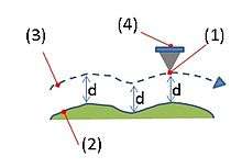
(1): Tip apex, (2): Sample surface, (3): Z-orbit of Tip apex, (4): Cantilever.
History
AFM was invented by IBM Scientists in 1982.The precursor to the AFM, the scanning tunneling microscope (STM), was developed by Gerd Binnig and Heinrich Rohrer in the early 1980s at IBM Research - Zurich, a development that earned them the Nobel Prize for Physics in 1986. Binnig invented[2] the atomic-force microscope and the first experimental implementation was made by Binnig, Quate and Gerber in 1986.[3]
The first commercially available atomic-force microscope was introduced in 1989. The AFM is one of the foremost tools for imaging, measuring, and manipulating matter at the nanoscale.
Applications
The AFM has been applied to problems in a wide range of disciplines of the natural sciences, including solid state physics, semiconductor science and technology, molecular engineering, polymer chemistry and physics, surface chemistry, molecular biology, cell biology and medicine.
Applications in the field of solid state physics include (a) the identification of atoms at a surface, (b) the evaluation of interactions between a specific atom and its neighboring atoms, and (c) the study of changes in physical properties arising from changes in an atomic arrangement through atomic manipulation.
In cellular biology, AFM can be used to (a) attempt to distinguish cancer cells and normal cells based on a hardness of cells, and (b) to evaluate interactions between a specific cell and its neighboring cells in a competitive culture system.
In some variations, electric potentials can also be scanned using conducting cantilevers. In more advanced versions, currents can be passed through the tip to probe the electrical conductivity or transport of the underlying surface, but this is a challenging task with few research groups reporting consistent data (as of 2004).[4]
Principles
_cantilever_in_Scanning_Electron_Microscope%2C_magnification_1000x.JPG)
_cantilever_in_Scanning_Electron_Microscope%2C_magnification_3000x.JPG)
The AFM consists of a cantilever with a sharp tip (probe) at its end that is used to scan the specimen surface. The cantilever is typically silicon or silicon nitride with a tip radius of curvature on the order of nanometers. When the tip is brought into proximity of a sample surface, forces between the tip and the sample lead to a deflection of the cantilever according to Hooke's law.[5] Depending on the situation, forces that are measured in AFM include mechanical contact force, van der Waals forces, capillary forces, chemical bonding, electrostatic forces, magnetic forces (see magnetic force microscope, MFM), Casimir forces, solvation forces, etc. Along with force, additional quantities may simultaneously be measured through the use of specialized types of probes (see scanning thermal microscopy, scanning joule expansion microscopy, photothermal microspectroscopy, etc.).

The AFM can be operated in a number of modes, depending on the application. In general, possible imaging modes are divided into static (also called contact) modes and a variety of dynamic (non-contact or "tapping") modes where the cantilever is vibrated or oscillated at a given frequency.[6]
Imaging modes
AFM operation is usually described as one of three modes, according to the nature of the tip motion: contact mode, also called static mode (as opposed to the other two modes, which are called dynamic modes); tapping mode, also called intermittent contact, AC mode, or vibrating mode, or, after the detection mechanism, amplitude modulation AFM; non-contact mode, or, again after the detection mechanism, frequency modulation AFM.
It should be noted that despite the nomenclature, repulsive contact can occur or be avoided both in amplitude modulation AFM and frequency modulation AFM, depending on the settings.
Contact mode
In contact mode, the tip is "dragged" across the surface of the sample and the contours of the surface are measured either using the deflection of the cantilever directly or, more commonly, using the feedback signal required to keep the cantilever at a constant position. Because the measurement of a static signal is prone to noise and drift, low stiffness cantilevers (i.e. cantilevers with a low spring constant, k) are used to achieve a large enough deflection signal while keeping the interaction force low. Close to the surface of the sample, attractive forces can be quite strong, causing the tip to "snap-in" to the surface. Thus, contact mode AFM is almost always done at a depth where the overall force is repulsive, that is, in firm "contact" with the solid surface.
Tapping mode
In ambient conditions, most samples develop a liquid meniscus layer. Because of this, keeping the probe tip close enough to the sample for short-range forces to become detectable while preventing the tip from sticking to the surface presents a major problem for non-contact dynamic mode in ambient conditions. Dynamic contact mode (also called intermittent contact, AC mode or tapping mode) was developed to bypass this problem.[8] Nowadays, tapping mode is the most frequently used AFM mode when operating in ambient conditions or in liquids.
In tapping mode, the cantilever is driven to oscillate up and down at or near its resonance frequency. This oscillation is commonly achieved with a small piezo element in the cantilever holder, but other possibilities include an AC magnetic field (with magnetic cantilevers), piezoelectric cantilevers, or periodic heating with a modulated laser beam. The amplitude of this oscillation usually varies from several nm to 200 nm. In tapping mode, the frequency and amplitude of the driving signal are kept constant, leading to a constant amplitude of the cantilever oscillation as long as there is no drift or interaction with the surface. The interaction of forces acting on the cantilever when the tip comes close to the surface, Van der Waals forces, dipole-dipole interactions, electrostatic forces, etc. cause the amplitude of the cantilever's oscillation to change (usually decrease) as the tip gets closer to the sample. This amplitude is used as the parameter that goes into the electronic servo that controls the height of the cantilever above the sample. The servo adjusts the height to maintain a set cantilever oscillation amplitude as the cantilever is scanned over the sample. A tapping AFM image is therefore produced by imaging the force of the intermittent contacts of the tip with the sample surface.[9]
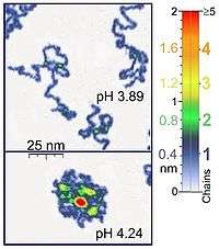
Although the peak forces applied during the contacting part of the oscillation can be much higher than typically used in contact mode, tapping mode generally lessens the damage done to the surface and the tip compared to the amount done in contact mode. This can be explained by the short duration of the applied force, and because the lateral forces between tip and sample are significantly lower in tapping mode over contact mode. Tapping mode imaging is gentle enough even for the visualization of supported lipid bilayers or adsorbed single polymer molecules (for instance, 0.4 nm thick chains of synthetic polyelectrolytes) under liquid medium. With proper scanning parameters, the conformation of single molecules can remain unchanged for hours,[7] and even single molecular motors can be imaged while moving.
When operating in tapping mode, the phase of the cantilever's oscillation with respect to the driving signal can be recorded as well. This signal channel contains information about the energy dissipated by the cantilever in each oscillation cycle. Samples that contain regions of varying stiffness or with different adhesion properties can give a contrast in this channel that is not visible in the topographic image. Extracting the sample's material properties in a quantitative manner from phase images, however, is often not feasible.
Non-contact mode
In non-contact atomic force microscopy mode, the tip of the cantilever does not contact the sample surface. The cantilever is instead oscillated at either its resonant frequency (frequency modulation) or just above (amplitude modulation) where the amplitude of oscillation is typically a few nanometers (<10 nm) down to a few picometers.[10] The van der Waals forces, which are strongest from 1 nm to 10 nm above the surface, or any other long-range force that extends above the surface acts to decrease the resonance frequency of the cantilever. This decrease in resonant frequency combined with the feedback loop system maintains a constant oscillation amplitude or frequency by adjusting the average tip-to-sample distance. Measuring the tip-to-sample distance at each (x,y) data point allows the scanning software to construct a topographic image of the sample surface.
Non-contact mode AFM does not suffer from tip or sample degradation effects that are sometimes observed after taking numerous scans with contact AFM. This makes non-contact AFM preferable to contact AFM for measuring soft samples, e.g. biological samples and organic thin film. In the case of rigid samples, contact and non-contact images may look the same. However, if a few monolayers of adsorbed fluid are lying on the surface of a rigid sample, the images may look quite different. An AFM operating in contact mode will penetrate the liquid layer to image the underlying surface, whereas in non-contact mode an AFM will oscillate above the adsorbed fluid layer to image both the liquid and surface.
Schemes for dynamic mode operation include frequency modulation where a phase-locked loop is used to track the cantilever's resonance frequency and the more common amplitude modulation with a servo loop in place to keep the cantilever excitation to a defined amplitude. In frequency modulation, changes in the oscillation frequency provide information about tip-sample interactions. Frequency can be measured with very high sensitivity and thus the frequency modulation mode allows for the use of very stiff cantilevers. Stiff cantilevers provide stability very close to the surface and, as a result, this technique was the first AFM technique to provide true atomic resolution in ultra-high vacuum conditions.[11]
In amplitude modulation, changes in the oscillation amplitude or phase provide the feedback signal for imaging. In amplitude modulation, changes in the phase of oscillation can be used to discriminate between different types of materials on the surface. Amplitude modulation can be operated either in the non-contact or in the intermittent contact regime. In dynamic contact mode, the cantilever is oscillated such that the separation distance between the cantilever tip and the sample surface is modulated.
Amplitude modulation has also been used in the non-contact regime to image with atomic resolution by using very stiff cantilevers and small amplitudes in an ultra-high vacuum environment.
Topographic image
Image formation is a plotting method that produces a color mapping through changing the x-y position of the tip while scanning and recording the measured variable, i.e. the intensity of control signal, to each x-y coordinate. The color mapping shows the measured value corresponding to each coordinate. The image expresses the intensity of a value as a hue. Usually, the correspondence between the intensity of a value and a hue is shown as a color scale in the explanatory notes accompanying the image.
What is the topographic image of atomic-force microscope?
Operation mode of Image forming of the AFM are generally classified into two groups from the viewpoint whether it uses z-Feedback loop (not shown) to maintain the tip-sample distance to keep signal intensity exported by the detector. The first one (using z-Feedback loop), said to be "constant XX mode" (XX is something which kept by z-Feedback loop).
Topographic Image Formation Mode is based on abovementioned "constant XX mode", z-Feedback loop controls the relative distance between the probe and the sample through outputting control signals to keep constant one of frequency, vibration and phase which typically corresponds to the motion of cantilever (for instance, voltage is applied to the Z-piezoelectric element and it moves the sample up and down towards the Z direction.
Details will be explained in the case that especially "constant df mode"(FM-AFM) among AFM as an instance in next section.
Topographic image of FM-AFM
When the distance between the probe and the sample is brought to the range where atomic force may be detected, while a cantilever is excited in its natural eigen frequency (f0), a phenomenon that the resonance frequency (f) of the cantilever shifts from the original resonance frequency (natural eigen frequency) of the cantilever. In other words, in the range where atomic force may be detected, the frequency shift (df=f-f0) will be observed. So, when the distance between the probe and the sample is in the non-contact region, the frequency shift increases in negative direction as the distance between the probe and the sample gets smaller.
When the sample has concavity and convexity, the distance between the tip-apex and the sample varies in accordance with the concavity and convexity accompanied with a scan of the sample along x-y direction (without height regulation in z-direction) . As a result, the frequency shift arises. The image in which the values of the frequency obtained by a raster scan along the x-y direction of the sample surface are plotted against the x-y coordination of each measurement point is called a constant-height image.
On the other hand, the df may be kept constant by moving the probe upward and downward (See (3) of FIG.5) in z-direction using a negative feedback (by using z-feedback loop) while the raster scan of the sample surface along the x-y direction . The image in which the amounts of the negative feedback (the moving distance of the probe upward and downward in z-direction) are plotted against the x-y coordination of each measurement point is a topographic image. In other words, the topographic image is a trace of the tip of the probe regulated so that the df is constant and it may also be considered to be a plot of a constant-height surface of the df.
Therefore, the topographic image of the AFM is not the exact surface morphology itself, but actually the image influenced by the bond-order between the probe and the sample, however, the topographic image of the AFM is considered to reflect the geographical shape of the surface more than the topographic image of a scanning tunnel microscope.
Force spectroscopy
Another major application of AFM (besides imaging) is force spectroscopy, the direct measurement of tip-sample interaction forces as a function of the gap between the tip and sample (the result of this measurement is called a force-distance curve). For this method, the AFM tip is extended towards and retracted from the surface as the deflection of the cantilever is monitored as a function of piezoelectric displacement. These measurements have been used to measure nanoscale contacts, atomic bonding, Van der Waals forces, and Casimir forces, dissolution forces in liquids and single molecule stretching and rupture forces.[12] Furthermore, AFM was used to measure, in an aqueous environment, the dispersion force due to polymer adsorbed on the substrate.[13] Forces of the order of a few piconewtons can now be routinely measured with a vertical distance resolution of better than 0.1 nanometers. Force spectroscopy can be performed with either static or dynamic modes. In dynamic modes, information about the cantilever vibration is monitored in addition to the static deflection.[14]
Problems with the technique include no direct measurement of the tip-sample separation and the common need for low-stiffness cantilevers, which tend to 'snap' to the surface. These problems are not insurmountable. An AFM that directly measures the tip-sample separation has been developed.[15] The snap-in can be reduced by measuring in liquids or by using stiffer cantilevers, but in the latter case a more sensitive deflection sensor is needed. By applying a small dither to the tip, the stiffness (force gradient) of the bond can be measured as well.[16]
Biological applications and other
Force spectroscopy is used in biophysics to measure the mechanical properties of living material (such as tissue or cells).[17][18] Another application was to measure the interaction forces between from one hand a material stuck on the tip of the cantilever, and from another hand the surface of particles either free or occupied by the same material. From the adhesion force distribution curve, a mean value of the forces has been derived. It allowed to make a cartography of the surface of the particles, covered or not by the material.[19]
Identification of individual surface atoms
The AFM can be used to image and manipulate atoms and structures on a variety of surfaces. The atom at the apex of the tip "senses" individual atoms on the underlying surface when it forms incipient chemical bonds with each atom. Because these chemical interactions subtly alter the tip's vibration frequency, they can be detected and mapped. This principle was used to distinguish between atoms of silicon, tin and lead on an alloy surface, by comparing these 'atomic fingerprints' to values obtained from large-scale density functional theory (DFT) simulations.[20]
The trick is to first measure these forces precisely for each type of atom expected in the sample, and then to compare with forces given by DFT simulations. The team found that the tip interacted most strongly with silicon atoms, and interacted 24% and 41% less strongly with tin and lead atoms, respectively. Thus, each different type of atom can be identified in the matrix as the tip is moved across the surface.
Probe
An AFM probe has a sharp tip on the free-swinging end of a cantilever that is protruding from a holder.[21] The dimensions of the cantilever are in the scale of micrometers. The radius of the tip is usually on the scale of a few nanometers to a few tens of nanometers. (Specialized probes exist with much larger end radii, for example probes for indentation of soft materials.) The cantilever holder, also called holder chip – often 1.6 mm by 3.4 mm in size – allows the operator to hold the AFM cantilever/probe assembly with tweezers and fit it into the corresponding holder clips on the scanning head of the atomic-force microscope.
This device is most commonly called an "AFM probe", but other names include "AFM tip" and "cantilever" (employing the name of a single part as the name of the whole device). An AFM probe is a particular type of SPM (scanning probe microscopy) probe.
AFM probes are manufactured with MEMS technology. Most AFM probes used are made from silicon (Si), but borosilicate glass and silicon nitride are also in use. AFM probes are considered consumables as they are often replaced when the tip apex becomes dull or contaminated or when the cantilever is broken. They can cost from a couple of tens of dollars up to hundreds of dollars per cantilever for the most specialized cantilever/probe combinations.
Just the tip is brought very close to the surface of the object under investigation, the cantilever is deflected by the interaction between the tip and the surface, which is what the AFM is designed to measure. A spatial map of the interaction can be made by measuring the deflection at many points on a 2D surface.
Several types of interaction can be detected. Depending on the interaction under investigation, the surface of the tip of the AFM probe needs to be modified with a coating. Among the coatings used are gold – for covalent bonding of biological molecules and the detection of their interaction with a surface,[22] diamond for increased wear resistance[23] and magnetic coatings for detecting the magnetic properties of the investigated surface.[24] Another solution exists to achieve high resolution magnetic imaging : having the probe equip with a microSQUID. The AFM tips is fabricated using silicon micro machining and the precise positioning of the microSQUID loop is done by electron beam lithography.[25]
The surface of the cantilevers can also be modified. These coatings are mostly applied in order to increase the reflectance of the cantilever and to improve the deflection signal.
AFM cantilever-deflection measurement
Beam-deflection measurement

r (PSD) consisting of two closely spaced photodiodes whose output signal is collected by a differential amplifier. Angular displacement of the cantilever results in one photodiode collecting more light than the other photodiode, producing an output signal (the difference between the photodiode signals normalized by their sum), which is proportional to the deflection of the cantilever. The sensitivity of the beam-deflection method is very high, a noise floor on the order of 10 fm Hz− 1⁄2 can be obtained routinely in a well-designed system. Although this method is sometimes called the 'optical lever' method, the signal is not amplified if the beam path is made longer. A longer beam path increases the motion of the reflected spot on the photodiodes, but also widens the spot by the same amount due to diffraction, so that the same amount of optical power is moved from one photodiode to the other. The 'optical leverage' (output signal of the detector divided by deflection of the cantilever) is inversely proportional to the numerical aperture of the beam focusing optics, as long as the focused laser spot is small enough to fall completely on the cantilever. It is also inversely proportional to the length of the cantilever. The most common method for cantilever-deflection measurements is the beam-deflection method. In this method, laser light from a solid-state diode is reflected off the back of the cantilever and collected by a position-sensitive detecto
The relative popularity of the beam-deflection method can be explained by its high sensitivity and simple operation, and by the fact that cantilevers do not require electrical contacts or other special treatments, and can therefore be fabricated relatively cheaply with sharp integrated tips.
Other deflection-measurement methods
Many other methods for beam-deflection measurements exist.
- Piezoelectric detection – Cantilevers made from quartz[26] (such as the qPlus configuration), or other piezoelectric materials can directly detect deflection as an electrical signal. Cantilever oscillations down to 10pm have been detected with this method.
- Laser Doppler vibrometry – A laser Doppler vibrometer can be used to produce very accurate deflection measurements for an oscillating cantilever[27] (thus is only used in non-contact mode). This method is expensive and is only used by relatively few groups.
- STM — The first atomic microscope used an STM complete with its own feedback mechanism to measure deflection.[6] This method is very difficult to implement, and is slow to react to deflection changes compared to modern methods.
- Optical interferometry – Optical interferometry can be used to measure cantilever deflection.[28] Due to the nanometre scale deflections measured in AFM, the interferometer is running in the sub-fringe regime, thus, any drift in laser power or wavelength has strong effects on the measurement. For these reasons optical interferometer measurements must be done with great care (for example using index matching fluids between optical fibre junctions), with very stable lasers. For these reasons optical interferometry is rarely used.
- Capacitive detection – Metal coated cantilevers can form a capacitor with another contact located behind the cantilever.[29] Deflection changes the distance between the contacts and can be measured as a change in capacitance.
- Piezoresistive detection – Cantilevers can be fabricated with piezoresistive elements that act as a strain gauge. Using a Wheatstone bridge, strain in the AFM cantilever due to deflection can be measured.[30] This is not commonly used in vacuum applications, as the piezoresistive detection dissipates energy from the system affecting Q of the resonance.
Piezoelectric scanners
AFM scanners are made from piezoelectric material, which expands and contracts proportionally to an applied voltage. Whether they elongate or contract depends upon the polarity of the voltage applied. Traditionally the tip or sample is mounted on a 'tripod' of three piezo crystals, with each responsible for scanning in the x,y and z directions.[6] In 1986, the same year as the AFM was invented, a new piezoelectric scanner, the tube scanner, was developed for use in STM.[31] Later tube scanners were incorporated into AFMs. The tube scanner can move the sample in the x, y, and z directions using a single tube piezo with a single interior contact and four external contacts. An advantage of the tube scanner compared to the original tripod design, is better vibrational isolation, resulting from the higher resonant frequency of the single element construction, in combination with a low resonant frequency isolation stage. A disadvantage is that the x-y motion can cause unwanted z motion resulting in distortion. Another popular design for AFM scanners is the flexure stage, which uses separate piezos for each axis, and couples them through a flexure mechanism.
Scanners are characterized by their sensitivity, which is the ratio of piezo movement to piezo voltage, i.e., by how much the piezo material extends or contracts per applied volt. Because of differences in material or size, the sensitivity varies from scanner to scanner. Sensitivity varies non-linearly with respect to scan size. Piezo scanners exhibit more sensitivity at the end than at the beginning of a scan. This causes the forward and reverse scans to behave differently and display hysteresis between the two scan directions.[32] This can be corrected by applying a non-linear voltage to the piezo electrodes to cause linear scanner movement and calibrating the scanner accordingly.[32] One disadvantage of this approach is that it requires re-calibration because the precise non-linear voltage needed to correct non-linear movement will change as the piezo ages (see below). This problem can be circumvented by adding a linear sensor to the sample stage or piezo stage to detect the true movement of the piezo. Deviations from ideal movement can be detected by the sensor and corrections applied to the piezo drive signal to correct for non-linear piezo movement. This design is known as a 'closed loop' AFM. Non-sensored piezo AFMs are referred to as 'open loop' AFMs.
The sensitivity of piezoelectric materials decreases exponentially with time. This causes most of the change in sensitivity to occur in the initial stages of the scanner's life. Piezoelectric scanners are run for approximately 48 hours before they are shipped from the factory so that they are past the point where they may have large changes in sensitivity. As the scanner ages, the sensitivity will change less with time and the scanner would seldom require recalibration,[33][34] though various manufacturer manuals recommend monthly to semi-monthly calibration of open loop AFMs.
Advantages and disadvantages
Just like any other tool, an AFM's usefulness has limitations. When determining whether or not analyzing a sample with an AFM is appropriate, there are various advantages and disadvantages that must be considered.
Advantages
AFM has several advantages over the scanning electron microscope (SEM). Unlike the electron microscope, which provides a two-dimensional projection or a two-dimensional image of a sample, the AFM provides a three-dimensional surface profile. In addition, samples viewed by AFM do not require any special treatments (such as metal/carbon coatings) that would irreversibly change or damage the sample, and does not typically suffer from charging artifacts in the final image. While an electron microscope needs an expensive vacuum environment for proper operation, most AFM modes can work perfectly well in ambient air or even a liquid environment. This makes it possible to study biological macromolecules and even living organisms. In principle, AFM can provide higher resolution than SEM. It has been shown to give true atomic resolution in ultra-high vacuum (UHV) and, more recently, in liquid environments. High resolution AFM is comparable in resolution to scanning tunneling microscopy and transmission electron microscopy. AFM can also be combined with a variety of optical microscopy techniques such as fluorescent microscopy, further expanding its applicability. Combined AFM-optical instruments have been applied primarily in the biological sciences but have also found a niche in some materials applications, especially those involving photovoltaics research.[9]
Disadvantages
A disadvantage of AFM compared with the scanning electron microscope (SEM) is the single scan image size. In one pass, the SEM can image an area on the order of square millimeters with a depth of field on the order of millimeters, whereas the AFM can only image a maximum scanning area of about 150×150 micrometers and a maximum height on the order of 10-20 micrometers. One method of improving the scanned area size for AFM is by using parallel probes in a fashion similar to that of millipede data storage.
The scanning speed of an AFM is also a limitation. Traditionally, an AFM cannot scan images as fast as an SEM, requiring several minutes for a typical scan, while an SEM is capable of scanning at near real-time, although at relatively low quality. The relatively slow rate of scanning during AFM imaging often leads to thermal drift in the image[35][36][37] making the AFM less suited for measuring accurate distances between topographical features on the image. However, several fast-acting designs[38][39] were suggested to increase microscope scanning productivity including what is being termed videoAFM (reasonable quality images are being obtained with videoAFM at video rate: faster than the average SEM). To eliminate image distortions induced by thermal drift, several methods have been introduced.[35][36][37]
AFM images can also be affected by nonlinearity, hysteresis,[32] and creep of the piezoelectric material and cross-talk between the x, y, z axes that may require software enhancement and filtering. Such filtering could "flatten" out real topographical features. However, newer AFMs utilize real-time correction software (for example, feature-oriented scanning[33][35]) or closed-loop scanners, which practically eliminate these problems. Some AFMs also use separated orthogonal scanners (as opposed to a single tube), which also serve to eliminate part of the cross-talk problems.
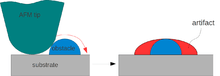
As with any other imaging technique, there is the possibility of image artifacts, which could be induced by an unsuitable tip, a poor operating environment, or even by the sample itself, as depicted on the right. These image artifacts are unavoidable; however, their occurrence and effect on results can be reduced through various methods. Artifacts resulting from a too-coarse tip can be caused for example by inappropriate handling or de facto collisions with the sample by either scanning too fast or having an unreasonably rough surface, causing actual wearing of the tip.

Due to the nature of AFM probes, they cannot normally measure steep walls or overhangs. Specially made cantilevers and AFMs can be used to modulate the probe sideways as well as up and down (as with dynamic contact and non-contact modes) to measure sidewalls, at the cost of more expensive cantilevers, lower lateral resolution and additional artifacts.
Other applications in various fields of study
The latest efforts in integrating nanotechnology and biological research have been successful and show much promise for the future. Since nanoparticles are a potential vehicle of drug delivery, the biological responses of cells to these nanoparticles are continuously being explored to optimize their efficacy and how their design could be improved.[40] Pyrgiotakis et al. were able to study the interaction between CeO2 and Fe2O3 engineered nanoparticles and cells by attaching the engineered nanoparticles to the AFM tip.[41] Beyond the interactions with external synthetic materials, cells have been imaged with X-ray crystallography and there has been much curiosity about their behavior in vivo. Studies have taken advantage of AFM to obtain further information on the behavior of live cells in biological media. Real-time atomic force spectroscopy (or nanoscopy) and dynamic atomic force spectroscopy have been used to study live cells and membrane proteins and their dynamic behavior at high resolution, on the nanoscale. Imaging and obtaining information on the topography and the properties of the cells has also given insight into chemical processes and mechanisms that occur through cell-cell interaction and interactions with other signaling molecules (ex. ligands). Evans and Calderwood used single cell force microscopy to study cell adhesion forces, bond kinetics/dynamic bond strength and its role in chemical processes such as cell signaling.[42] Scheuring, Lévy, and Rigaud reviewed studies in which AFM to explore the crystal structure of membrane proteins of photosynthetic bacteria.[43] Alsteen et al. have used AFM-based nanoscopy to perform a real-time analysis of the interaction between live mycobacteria and antimycobacterial drugs (specifically isoniazid, ethionamide, ethambutol, and streptomycine),[44] which serves as an example of the more in-depth analysis of pathogen-drug interactions that can be done through AFM.
See also
References
- ↑ Sharifi-viand, Ahmad; Mahjani, Mohamad Ghasem; Moshrefi, Reza; Jafarian, Majid (April 2015). "Diffusion through the self-affine surface of polypyrrole film". Vacuum. 114: 17–20. Bibcode:2015Vacuu.114...17S. doi:10.1016/j.vacuum.2014.12.030.
- 1 2 Patent US4724318 - Atomic-force microscope and method for imaging surfaces with atomic resolution
- ↑ Binnig, G.; Quate, C. F.; Gerber, C. (1986). "Atomic-Force Microscope". Physical Review Letters. 56: 930–933. Bibcode:1986PhRvL..56..930B. doi:10.1103/physrevlett.56.930.
- ↑ Lang, K.M.; D. A. Hite; R. W. Simmonds; R. McDermott; D. P. Pappas; John M. Martinis (2004). "Conducting atomic-force microscopy for nanoscale tunnel barrier characterization". Review of Scientific Instruments. 75 (8): 2726–2731. Bibcode:2004RScI...75.2726L. doi:10.1063/1.1777388.
- ↑ Cappella, B; Dietler, G (1999). "Force-distance curves by atomic-force microscopy" (PDF). Surface Science Reports. 34 (1–3): 1–104. Bibcode:1999SurSR..34....1C. doi:10.1016/S0167-5729(99)00003-5. Archived from the original (PDF) on 2012-12-03.
- 1 2 3 Binnig, G.; Quate, C. F.; Gerber, Ch. (1986). "Atomic-Force Microscope". Physical Review Letters. 56 (9): 930–933. Bibcode:1986PhRvL..56..930B. doi:10.1103/PhysRevLett.56.930. ISSN 0031-9007. PMID 10033323.
- 1 2 Roiter, Y; Minko, S (Nov 2005). "AFM single molecule experiments at the solid-liquid interface: in situ conformation of adsorbed flexible polyelectrolyte chains". Journal of the American Chemical Society. 127 (45): 15688–9. doi:10.1021/ja0558239. ISSN 0002-7863. PMID 16277495.
- ↑ Zhong, Q; Inniss, D; Kjoller, K; Elings, V (1993). "Fractured polymer/silica fiber surface studied by tapping mode atomic-force microscopy". Surface Science Letters. 290: L688. Bibcode:1993SurSL.290L.688Z. doi:10.1016/0167-2584(93)90906-Y.
- 1 2 Geisse, Nicholas A. (July–August 2009). "AFM and Combined Optical Techniques". Materials Today. 12 (7–8): 40–45. doi:10.1016/S1369-7021(09)70201-9. Retrieved 4 November 2011.
- ↑ Gross, L.; Mohn, F.; Moll, N.; Liljeroth, P.; Meyer, G. (27 August 2009). "The Chemical Structure of a Molecule Resolved by Atomic-Force Microscopy". Science. 325 (5944): 1110–1114. Bibcode:2009Sci...325.1110G. doi:10.1126/science.1176210. PMID 19713523.
- ↑ Giessibl, Franz J. (2003). "Advances in atomic-force microscopy". Reviews of Modern Physics. 75 (3): 949–983. arXiv:cond-mat/0305119
 . Bibcode:2003RvMP...75..949G. doi:10.1103/RevModPhys.75.949.
 - ↑ Hinterdorfer, P; Dufrêne, Yf (May 2006). "Detection and localization of single molecular recognition events using atomic-force microscopy". Nature Methods. 3 (5): 347–55. doi:10.1038/nmeth871. ISSN 1548-7091. PMID 16628204.
- ↑ Ferrari, L.; Kaufmann, J.; Winnefeld, F.; Plank, J. (Jul 2010). "Interaction of cement model systems with superplasticizers investigated by atomic-force microscopy, zeta potential, and adsorption measurements". J Colloid Interface Sci. 347 (1): 15–24. doi:10.1016/j.jcis.2010.03.005. PMID 20356605.
- ↑ Butt, H; Cappella, B; Kappl, M (2005). "Force measurements with the atomic-force microscope: Technique, interpretation and applications". Surface Science Reports. 59: 1–152. Bibcode:2005SurSR..59....1B. doi:10.1016/j.surfrep.2005.08.003.
- ↑ Gavin M. King; Ashley R. Carter; Allison B. Churnside; Louisa S. Eberle & Thomas T. Perkins (2009). "Ultrastable Atomic-Force Microscopy: Atomic-Scale Stability and Registration in Ambient Conditions". Nano Letters. 9 (4): 1451–1456. Bibcode:2009NanoL...9.1451K. doi:10.1021/nl803298q. PMC 2953871. PMID 19351191.
- ↑ M. Hoffmann, Ahmet Oral; Ralph A. G, Peter (2001). "Direct measurement of interatomic-force gradients using an ultra-low-amplitude atomic-force microscope". Proceedings of the Royal Society A. 457 (2009): 1161–1174. Bibcode:2001RSPSA.457.1161M. doi:10.1098/rspa.2000.0713.
- ↑ Radmacher, M. (1997). "Measuring the elastic properties of biological samples with the AFM". IEEE Eng Med Biol Mag. 16 (2): 47–57. doi:10.1109/51.582176. PMID 9086372.
- ↑ Perkins, Thomas. "Atomic force microscopy measures properties of proteins and protein folding". SPIE Newsroom. Retrieved 4 March 2016.
- ↑ Thomas, G.; Y. Ouabbas; P. Grosseau; M. Baron; A. Chamayou; L. Galet (2009). "Modeling the mean interaction forces between power particles. Application to silice gel-magnesium stearate mixtures". Applied Surface Science. 255: 7500–7507. Bibcode:2009ApSS..255.7500T. doi:10.1016/j.apsusc.2009.03.099.
- ↑ Sugimoto, Y; Pou, P; Abe, M; Jelinek, P; Pérez, R; Morita, S; Custance, O (Mar 2007). "Chemical identification of individual surface atoms by atomic-force microscopy". Nature. 446 (7131): 64–7. Bibcode:2007Natur.446...64S. doi:10.1038/nature05530. ISSN 0028-0836. PMID 17330040.
- ↑ Bryant, P. J.; Miller, R. G.; Yang, R.; "Scanning tunneling and atomic-force microscopy combined". Applied Physics Letters, Jun 1988, Vol: 52 Issue:26, p. 2233–2235, ISSN 0003-6951.
- ↑ Oscar H. Willemsen, Margot M.E. Snel, Alessandra Cambi, Jan Greve, Bart G. De Grooth and Carl G. Figdor "Biomolecular Interactions Measured by Atomic Force Microscopy" Biophysical Journal, Volume 79, Issue 6, December 2000, Pages 3267-3281.
- ↑ Koo-Hyun Chung and Dae-Eun Kim, "Wear characteristics of diamond-coated atomic force microscope probe". Ultramicroscopy, Volume 108, Issue 1, December 2007, Pages 1-10
- ↑ Xu, Xin; Raman, Arvind (2007). "Comparative dynamics of magnetically, acoustically, and Brownian motion driven microcantilevers in liquids". J. Appl. Phys. 102: 034303. Bibcode:2007JAP...102a4303Y. doi:10.1063/1.2751415.
- ↑ Hasselbach, K.; Ladam, C. (2008). "High resolution magnetic imaging : MicroSQUID Force Microscopy". Journal of Physics: Conference Series. 97: 012330. Bibcode:2008JPhCS..97a2330H. doi:10.1088/1742-6596/97/1/012330.
- ↑ Giessibl, Franz J. (1 January 1998). "High-speed force sensor for force microscopy and profilometry utilizing a quartz tuning fork". Applied Physics Letters. 73 (26): 3956. Bibcode:1998ApPhL..73.3956G. doi:10.1063/1.122948.
- ↑ Nishida, Shuhei; Kobayashi, Dai; Sakurada, Takeo; Nakazawa, Tomonori; Hoshi, Yasuo; Kawakatsu, Hideki (1 January 2008). "Photothermal excitation and laser Doppler velocimetry of higher cantilever vibration modes for dynamic atomic-force microscopy in liquid". Review of Scientific Instruments. 79 (12): 123703. Bibcode:2008RScI...79l3703N. doi:10.1063/1.3040500. PMID 19123565.
- ↑ Rugar, D.; Mamin, H. J.; Guethner, P. (1 January 1989). "Improved fiber-optic interferometer for atomic-force microscopy". Applied Physics Letters. 55 (25): 2588. Bibcode:1989ApPhL..55.2588R. doi:10.1063/1.101987.
- ↑ Göddenhenrich, T. "Force microscope with capacitive displacement detection". Journal of Vacuum Science and Technology A. 8 (1): 383. doi:10.1116/1.576401.
- ↑ Giessibl, F. J.; Trafas, B. M. (1 January 1994). "Piezoresistive cantilevers utilized for scanning tunneling and scanning force microscope in ultrahigh vacuum". Review of Scientific Instruments. 65 (6): 1923. Bibcode:1994RScI...65.1923G. doi:10.1063/1.1145232.
- ↑ Binnig, G.; Smith, D. P. E. (1986). "Single-tube three-dimensional scanner for scanning tunneling microscopy". Review of Scientific Instruments. 57 (8): 1688. Bibcode:1986RScI...57.1688B. doi:10.1063/1.1139196. ISSN 0034-6748.
- 1 2 3 R. V. Lapshin (1995). "Analytical model for the approximation of hysteresis loop and its application to the scanning tunneling microscope" (PDF). Review of Scientific Instruments. USA: AIP. 66 (9): 4718–4730. Bibcode:1995RScI...66.4718L. doi:10.1063/1.1145314. ISSN 0034-6748. (Russian translation is available).
- 1 2 R. V. Lapshin (2011). "Feature-oriented scanning probe microscopy". In H. S. Nalwa. Encyclopedia of Nanoscience and Nanotechnology (PDF). 14. USA: American Scientific Publishers. pp. 105–115. ISBN 1-58883-163-9.
- ↑ R. V. Lapshin (1998). "Automatic lateral calibration of tunneling microscope scanners" (PDF). Review of Scientific Instruments. USA: AIP. 69 (9): 3268–3276. Bibcode:1998RScI...69.3268L. doi:10.1063/1.1149091. ISSN 0034-6748.
- 1 2 3 R. V. Lapshin (2004). "Feature-oriented scanning methodology for probe microscopy and nanotechnology" (PDF). Nanotechnology. UK: IOP. 15 (9): 1135–1151. Bibcode:2004Nanot..15.1135L. doi:10.1088/0957-4484/15/9/006. ISSN 0957-4484.
- 1 2 R. V. Lapshin (2007). "Automatic drift elimination in probe microscope images based on techniques of counter-scanning and topography feature recognition" (PDF). Measurement Science and Technology. UK: IOP. 18 (3): 907–927. Bibcode:2007MeScT..18..907L. doi:10.1088/0957-0233/18/3/046. ISSN 0957-0233.
- 1 2 V. Y. Yurov; A. N. Klimov (1994). "Scanning tunneling microscope calibration and reconstruction of real image: Drift and slope elimination" (PDF). Review of Scientific Instruments. USA: AIP. 65 (5): 1551–1557. Bibcode:1994RScI...65.1551Y. doi:10.1063/1.1144890. ISSN 0034-6748.
- ↑ G. Schitter; M. J. Rost (2008). "Scanning probe microscopy at video-rate". Materials Today. UK: Elsevier. 11 (special issue): 40–48. doi:10.1016/S1369-7021(09)70006-9. ISSN 1369-7021. Archived from the original (PDF) on September 9, 2009.
- ↑ R. V. Lapshin; O. V. Obyedkov (1993). "Fast-acting piezoactuator and digital feedback loop for scanning tunneling microscopes" (PDF). Review of Scientific Instruments. USA: AIP. 64 (10): 2883–2887. Bibcode:1993RScI...64.2883L. doi:10.1063/1.1144377. ISSN 0034-6748.
- ↑ Jong, Wim H De; Borm, Paul JA (June 2008). "Drug Delivery and Nanoparticles: Applications and Hazards". Dovepress International Journal of Nanomedicine: 133–149.
- ↑ Pyrgiotakis, Georgios; Blattmann, Christoph O.; Demokritou, Philip (10 June 2014). "Real-Time Nanoparticle-Cell Interactions in Physiological Media by Atomic Force Microscopy". ACS Sustainable Chemistry & Engineering (Sustainable Nanotechnology 2013): 1681–1690.
- ↑ Evans, Evan A.; Calderwood, David A. (25 May 2007). "Forces and Bond Dynamics in Cell Adhesion". Science. 316 (5828): 1148–1153. Bibcode:2007Sci...316.1148E. doi:10.1126/science.1137592.
- ↑ Scheuring, Simon; Lévy, Daniel; Rigaud, Jean-Louis (1 July 2005). "Watching the Components". Elsevier. 1712 (2): 109–127. doi:10.1016/j.bbamem.2005.04.005.
- ↑ Alsteens, David; Verbelen, Claire; Dague, Etienne; Raze, Dominique; Baulard, Alain R.; Dufrêne, Yves F. (April 2008). "Organization of the Mycobacterial Cell Wall: A Nanoscale View". Pflügers Archive European Journal of Physiology. 456 (1): 117–125. doi:10.1007/s00424-007-0386-0.
Further reading
- Carpick, Robert W.; Salmeron, Miquel (1997). "Scratching the Surface: Fundamental Investigations of Tribology with Atomic Force Microscopy". Chemical Reviews. 97 (4): 1163–1194. doi:10.1021/cr960068q. ISSN 0009-2665.
- Giessibl, Franz J. (2003). "Advances in atomic force microscopy". Reviews of Modern Physics. 75 (3): 949–983. arXiv:cond-mat/0305119. Bibcode:2003RvMP...75..949G. doi:10.1103/RevModPhys.75.949. ISSN 0034-6861.
- Ricardo, Garcia; Knoll, Armin; Riedo, Elisa (2014). "Advanced Scanning Probe Lithography". Nature Nanotechnology. 9: 577. doi:10.1038/NNANO.2014.157.
External links
| Wikimedia Commons has media related to Atomic force microscopy. |
| Wikibooks has a book on the topic of: The Opensource Handbook of Nanoscience and Nanotechnology |
- List of AFM Instruments and Manufacturers (organized by filter options)
- SPM gallery: surface scans, collages, artworks, desktop wallpapers
- AFM Scan Image Gallery (organized by application area)
- Gwyddion: Multiplatform modular free software for visualization and analysis of AFM data