Photodiode
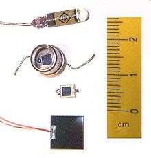
 Three Si and one Ge (top) photodiodes. | |
| Type | Passive |
|---|---|
| Working principle | Converts light into current |
| Pin configuration | anode and cathode |
| Electronic symbol | |
 | |

A photodiode is a semiconductor device that converts light into current. The current is generated when photons are absorbed in the photodiode. A small amount of current is also produced when no light is present. Photodiodes may contain optical filters, built-in lenses, and may have large or small surface areas. Photodiodes usually have a slower response time as their surface area increases. The common, traditional solar cell used to generate electric solar power is a large area photodiode.
Photodiodes are similar to regular semiconductor diodes except that they may be either exposed (to detect vacuum UV or X-rays) or packaged with a window or optical fiber connection to allow light to reach the sensitive part of the device. Many diodes designed for use specifically as a photodiode use a PIN junction rather than a p–n junction, to increase the speed of response. A photodiode is designed to operate in reverse bias.[1]
Principle of operation
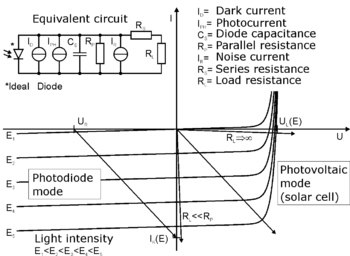
A photodiode is a p–n junction or PIN structure. When a photon of sufficient energy strikes the diode, it creates an electron-hole pair. This mechanism is also known as the inner photoelectric effect. If the absorption occurs in the junction's depletion region, or one diffusion length away from it, these carriers are swept from the junction by the built-in electric field of the depletion region. Thus holes move toward the anode, and electrons toward the cathode, and a photocurrent is produced. The total current through the photodiode is the sum of the dark current (current that is generated in the absence of light) and the photocurrent, so the dark current must be minimized to maximize the sensitivity of the device.[2]
Photovoltaic mode
When used in zero bias or photovoltaic mode, the flow of photocurrent out of the device is restricted and a voltage builds up. This mode exploits the photovoltaic effect, which is the basis for solar cells – a traditional solar cell is just a large area photodiode.
Photoconductive mode
In this mode the diode is often reverse biased (with the cathode driven positive with respect to the anode). This reduces the response time because the additional reverse bias increases the width of the depletion layer, which decreases the junction's capacitance. The reverse bias also increases the dark current without much change in the photocurrent. For a given spectral distribution, the photocurrent is linearly proportional to the illuminance (and to the irradiance).[3]
Although this mode is faster, the photoconductive mode tends to exhibit more electronic noise.[4] The leakage current of a good PIN diode is so low (<1 nA) that the Johnson–Nyquist noise of the load resistance in a typical circuit often dominates.
Other modes of operation
Avalanche photodiodes are photodiodes with structure optimized for operating with high reverse bias, approaching the reverse breakdown voltage. This allows each photo-generated carrier to be multiplied by avalanche breakdown, resulting in internal gain within the photodiode, which increases the effective responsivity of the device.

A phototransistor is a light-sensitive transistor. A common type of phototransistor, called a photobipolar transistor, is in essence a bipolar transistor encased in a transparent case so that light can reach the base–collector junction. It was invented by Dr. John N. Shive (more famous for his wave machine) at Bell Labs in 1948,[5]:205 but it was not announced until 1950.[6] The electrons that are generated by photons in the base–collector junction are injected into the base, and this photodiode current is amplified by the transistor's current gain β (or hfe). If the base and collector leads are used and the emitter is left unconnected, the phototransistor becomes a photodiode. While phototransistors have a higher responsivity for light they are not able to detect low levels of light any better than photodiodes. Phototransistors also have significantly longer response times. Field-effect phototransistors, also known as photoFETs, are light-sensitive field-effect transistors. Unlike photobipolar transistors, photoFETs control drain-source current by creating a gate voltage.
Materials
The material used to make a photodiode is critical to defining its properties, because only photons with sufficient energy to excite electrons across the material's bandgap will produce significant photocurrents.
Materials commonly used to produce photodiodes include:[7]
| Material | Electromagnetic spectrum wavelength range (nm) |
|---|---|
| Silicon | 190–1100 |
| Germanium | 400–1700 |
| Indium gallium arsenide | 800–2600 |
| Lead(II) sulfide | <1000–3500 |
| Mercury cadmium telluride | 400–14000 |
Because of their greater bandgap, silicon-based photodiodes generate less noise than germanium-based photodiodes.
Unwanted photodiode effects
Any p–n junction, if illuminated, is potentially a photodiode. Semiconductor devices such as transistors and ICs contain p–n junctions, and will not function correctly if they are illuminated by unwanted electromagnetic radiation (light) of wavelength suitable to produce a photocurrent;[8][9] this is avoided by encapsulating devices in opaque housings. If these housings are not completely opaque to high-energy radiation (ultraviolet, X-rays, gamma rays), transistors and ICs can malfunction[10] due to induced photo-currents. Background radiation from the packaging is also significant.[11] Radiation hardening mitigates these effects.
The infamous Raspberry Pi 2 xenon flash hanging bug, whereby the unit crashes when a flash photo is taken of it, is a result of the flash's intense ultraviolet emissions disrupting a switch mode power supply controller chip in bare-die wafer-scale package, with the resulting power surge causing the main processor to lock up.
Features
Critical performance parameters of a photodiode include:
- Responsivity
- The Spectral responsivity is a ratio of the generated photocurrent to incident light power, expressed in A/W when used in photoconductive mode. The wavelength-dependence may also be expressed as a Quantum efficiency, or the ratio of the number of photogenerated carriers to incident photons, a unitless quantity.
- Dark current
- The current through the photodiode in the absence of light, when it is operated in photoconductive mode. The dark current includes photocurrent generated by background radiation and the saturation current of the semiconductor junction. Dark current must be accounted for by calibration if a photodiode is used to make an accurate optical power measurement, and it is also a source of noise when a photodiode is used in an optical communication system.
- Response time
- A photon absorbed by the semiconducting material will generate an electron-hole pair which will in turn start moving in the material under the effect of the electric field and thus generate a current. The finite duration of this current is known as the transit-time spread and can be evaluated by using Ramo's theorem. One can also show with this theorem that the total charge generated in the external circuit is well e and not 2e as might seem by the presence of the two carriers. Indeed, the integral of the current due to both electron and hole over time must be equal to e. The resistance and capacitance of the photodiode and the external circuitry give rise to another response time known as RC time constant . This combination of R and C integrates the photoresponse over time and thus lengthens the impulse response of the photodiode. When used in an optical communication system, the response time determines the bandwidth available for signal modulation and thus data transmission.
- Noise-equivalent power
- (NEP) The minimum input optical power to generate photocurrent, equal to the rms noise current in a 1 hertz bandwidth. NEP is essentially the minimum detectable power. The related characteristic detectivity () is the inverse of NEP, 1/NEP. There is also the specific detectivity () which is the detectivity multiplied by the square root of the area () of the photodetector, () for a 1 Hz bandwidth. The specific detectivity allows different systems to be compared independent of sensor area and system bandwidth; a higher detectivity value indicates a low-noise device or system.[12] Although it is traditional to give () in many catalogues as a measure of the diode's quality, in practice, it is hardly ever the key parameter.
When a photodiode is used in an optical communication system, all these parameters contribute to the sensitivity of the optical receiver, which is the minimum input power required for the receiver to achieve a specified bit error rate.
Applications
P–n photodiodes are used in similar applications to other photodetectors, such as photoconductors, charge-coupled devices, and photomultiplier tubes. They may be used to generate an output which is dependent upon the illumination (analog; for measurement and the like), or to change the state of circuitry (digital; either for control and switching, or digital signal processing).
Photodiodes are used in consumer electronics devices such as compact disc players, smoke detectors, and the receivers for infrared remote control devices used to control equipment from televisions to air conditioners. For many applications either photodiodes or photoconductors may be used. Either type of photosensor may be used for light measurement, as in camera light meters, or to respond to light levels, as in switching on street lighting after dark.
Photosensors of all types may be used to respond to incident light, or to a source of light which is part of the same circuit or system. A photodiode is often combined into a single component with an emitter of light, usually a light-emitting diode (LED), either to detect the presence of a mechanical obstruction to the beam (slotted optical switch), or to couple two digital or analog circuits while maintaining extremely high electrical isolation between them, often for safety (optocoupler). The combination of LED and photodiode is also used in many sensor systems to characterize different types of products based on their optical absorbance.[13]
Photodiodes are often used for accurate measurement of light intensity in science and industry. They generally have a more linear response than photoconductors.
They are also widely used in various medical applications, such as detectors for computed tomography (coupled with scintillators), instruments to analyze samples (immunoassay), and pulse oximeters.
PIN diodes are much faster and more sensitive than p–n junction diodes, and hence are often used for optical communications and in lighting regulation.
P–n photodiodes are not used to measure extremely low light intensities. Instead, if high sensitivity is needed, avalanche photodiodes, intensified charge-coupled devices or photomultiplier tubes are used for applications such as astronomy, spectroscopy, night vision equipment and laser rangefinding.
Pinned photodiode is not a PIN photodiode, it has p+/n/p regions in it. It has a shallow P+ implant in N type diffusion layer over a P-type epitaxial substrate layer. It is used in CMOS Active pixel sensor.[14]
Comparison with photomultipliers
Advantages compared to photomultipliers:[15]
- Excellent linearity of output current as a function of incident light
- Spectral response from 190 nm to 1100 nm (silicon), longer wavelengths with other semiconductor materials
- Low noise
- Ruggedized to mechanical stress
- Low cost
- Compact and light weight
- Long lifetime
- High quantum efficiency, typically 60–80% [16]
- No high voltage required
Disadvantages compared to photomultipliers:
- Small area
- No internal gain (except avalanche photodiodes, but their gain is typically 102–103 compared to 105-108 for the photomultiplier)
- Much lower overall sensitivity
- Photon counting only possible with specially designed, usually cooled photodiodes, with special electronic circuits
- Response time for many designs is slower
- latent effect
Photodiode array

A one-dimensional array of hundreds or thousands of photodiodes can be used as a position sensor, for example as part of an angle sensor.[17] One advantage of photodiode arrays (PDAs) is that they allow for high speed parallel read out since the driving electronics may not be built in like a traditional CMOS or CCD sensor.
See also
- Electronics
- Band gap
- Infrared
- Optoelectronics
- Optical interconnect
- Light Peak
- Interconnect bottleneck
- Optical fiber cable
- Optical communication
- Parallel optical interface
- Opto-isolator
- Semiconductor device
- Solar cell
- Avalanche photodiode
- Transducer
- LEDs as Photodiode Light Sensors
- Light meter
- Image sensor
- Transimpedance amplifier
References
![]() This article incorporates public domain material from the General Services Administration document "Federal Standard 1037C".
This article incorporates public domain material from the General Services Administration document "Federal Standard 1037C".
- ↑ Cox, James F. (2001). Fundamentals of linear electronics: integrated and discrete. Cengage Learning. pp. 91–. ISBN 978-0-7668-3018-9.
- ↑ Tavernier, Filip and Steyaert, Michiel (2011) High-Speed Optical Receivers with Integrated Photodiode in Nanoscale CMOS. Springer. ISBN 1-4419-9924-8. Chapter 3 From Light to Electric Current – The Photodiode
- ↑ "Photodiode slide". hyperphysics.phy-astr.gsu.edu.
- ↑ "Photodiode Application Notes – Excelitas – see note 4" (PDF).
- ↑ Riordan, Michael and Hoddeson, Lillian (1998). Crystal Fire: The Invention of the Transistor and the Birth of the Information Age. ISBN 9780393318517.
- ↑ "The phototransistor". Bell Laboratories RECORD. May 1950.
- ↑ Held. G, Introduction to Light Emitting Diode Technology and Applications, CRC Press, (Worldwide, 2008). Ch. 5 p. 116. ISBN 1-4200-7662-0
- ↑ Shanfield, Z. et al (1988) Investigation of radiation effects on semiconductor devices and integrated circuits, DNA-TR-88-221
- ↑ Iniewski, Krzysztof (ed.) (2010), Radiation Effects in Semiconductors, CRC Press, ISBN 978-1-4398-2694-2
- ↑ Zeller, H.R. (1995). "Cosmic ray induced failures in high power semiconductor devices". Solid-State Electronics. 38 (12): 2041–2046. doi:10.1016/0038-1101(95)00082-5.
- ↑ May, T.C.; Woods, M.H. (1979). "Alpha-particle-induced soft errors in dynamic memories". IEEE Transactions on Electron Devices. 26: 2. doi:10.1109/T-ED.1979.19370. Cited in Baumann, R. C. (2004). "Soft errors in commercial integrated circuits". International Journal of High Speed Electronics and Systems. 14 (2): 299. doi:10.1142/S0129156404002363.
alpha particles emitted from the natural radioactive decay of uranium, thorium, and aughter isotopes present as impurities in packaging materials were found to be the dominant cause of [soft error rate] in [dynamic random-access memories].
- ↑ Brooker, Graham (2009) Introduction to Sensors for Ranging and Imaging, ScitTech Publishing. p. 87. ISBN 9781891121746
- ↑ Grossi, Marco; Di Lecce, Giuseppe; Arru, Marco; Gallina Toschi, Tullia; Riccò, Bruno (2015). "An opto-electronic system for in-situ determination of peroxide value and total phenol content in olive oil". Journal of Food Engineering. 146: 1–7. doi:10.1016/j.jfoodeng.2014.08.015.
- ↑ Difference between Buried Photodiode and Pinned Photodiode. stackexchange.com
- ↑ Photodiode Technical Guide on Hamamatsu website
- ↑ Knoll, F.G. (2010). Radiation detection and measurement, 4th ed. Wiley, Hoboken, NJ. p. 298. ISBN 978-0-470-13148-0
- ↑ Gao, Wei (2010). Precision Nanometrology: Sensors and Measuring Systems for Nanomanufacturing. Springer. pp. 15–16. ISBN 978-1-84996-253-7.
External links
| Wikimedia Commons has media related to Photodiodes. |
- Hamamatsu Application Note
- Using the Photodiode to convert the PC to a Light Intensity Logger
- Design Fundamentals for Phototransistor Circuits
- Working principles of photodiodes
- Excelitas Application Notes on Pacer Website